8086
Table 1. Pin Description
The following pin function descriptions are for 8086 systems in either minimum or maximum mode. The ‘‘Local
Bus’’ in these descriptions is the direct multiplexed bus interface connection to the 8086 (without regard to
additional bus buffers).
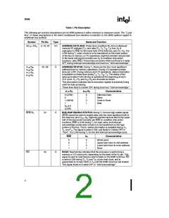
Symbol
AD –AD
Pin No.
Type
Name and Function
2–16, 39
I/O
ADDRESS DATA BUS: These lines constitute the time multiplexed
memory/IO address (T ), and data (T , T , T , T ) bus. A is
15
0
1
2
3
W
analogous to BHE for the lower byte of the data bus, pins D –D . It is
4
0
7
0
LOW during T when a byte is to be transferred on the lower portion
1
of the bus in memory or I/O operations. Eight-bit oriented devices tied
to the lower half would normally use A to condition chip select
0
functions. (See BHE.) These lines are active HIGH and float to 3-state
OFF during interrupt acknowledge and local bus ‘‘hold acknowledge’’.
A
19
A
18
A
17
A
16
/S ,
35–38
O
ADDRESS/STATUS: During T these are the four most significant
1
6
/S ,
address lines for memory operations. During I/O operations these
lines are LOW. During memory and I/O operations, status information
is available on these lines during T , T , T , T . The status of the
5
/S ,
4
/S
2
3
W
4
3
interrupt enable FLAG bit (S ) is updated at the beginning of each
5
CLK cycle. A /S and A /S are encoded as shown.
17
4
16
3
This information indicates which relocation register is presently being
used for data accessing.
These lines float to 3-state OFF during local bus ‘‘hold acknowledge.’’
A /S
17
A /S
16 3
Characteristics
4
0 (LOW)
0
0
Alternate Data
Stack
1
0
1
1 (HIGH)
1
Code or None
Data
S
is 0
(LOW)
6
BHE/S
34
O
BUS HIGH ENABLE/STATUS: During T the bus high enable signal
7
1
(BHE) should be used to enable data onto the most significant half of
the data bus, pins D –D . Eight-bit oriented devices tied to the upper
15
8
half of the bus would normally use BHE to condition chip select
functions. BHE is LOW during T for read, write, and interrupt
1
acknowledge cycles when a byte is to be transferred on the high
portion of the bus. The S status information is available during T ,
2
7
T , and T . The signal is active LOW, and floats to 3-state OFF in
3
4
‘‘hold’’. It is LOW during T for the first interrupt acknowledge cycle.
1
BHE
A
Characteristics
0
0
0
1
1
0
Whole word
1
0
1
Upper byte from/to odd address
Lower byte from/to even address
None
RD
32
O
READ: Read strobe indicates that the processor is performing a
memory or I/O read cycle, depending on the state of the S pin. This
2
signal is used to read devices which reside on the 8086 local bus. RD
is active LOW during T , T and T of any read cycle, and is
2
3
W
guaranteed to remain HIGH in T until the 8086 local bus has floated.
2
This signal floats to 3-state OFF in ‘‘hold acknowledge’’.
2

 INTEL [ INTEL ]