8086
ABSOLUTE MAXIMUM RATINGS*
NOTICE: This is a production data sheet. The specifi-
cations are subject to change without notice.
Ambient Temperature Under Bias ¿¿¿¿¿¿0 C to 70 C
ß
ß
Storage Temperature ¿¿¿¿¿¿¿¿¿¿ 65 C to 150 C
*WARNING: Stressing the device beyond the ‘‘Absolute
Maximum Ratings’’ may cause permanent damage.
These are stress ratings only. Operation beyond the
‘‘Operating Conditions’’ is not recommended and ex-
tended exposure beyond the ‘‘Operating Conditions’’
may affect device reliability.
b
a
ß
ß
Voltage on Any Pin with
Respect to Ground¿¿¿¿¿¿¿¿¿¿¿¿¿¿ 1.0V to 7V
b
a
Power Dissipation¿¿¿¿¿¿¿¿¿¿¿¿¿¿¿¿¿¿¿¿¿¿¿¿¿¿2.5W
e
e
e
e
e
e
g
5V 10%)
g
5V 5%)
g
5V 5%)
D.C. CHARACTERISTICS (8086:
T
(8086-1: T
0 C to 70 C, V
ß
ß
A
A
A
CC
CC
CC
0 C to 70 C, V
ß
ß
(8086-2: T
0 C to 70 C, V
ß ß
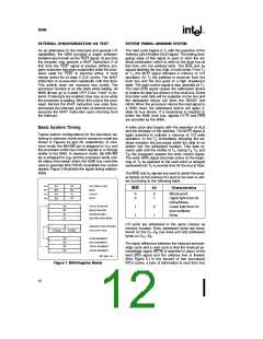
Symbol
Parameter
Input Low Voltage
Input High Voltage
Output Low Voltage
Output High Voltage
Min
Max
Units
Test Conditions
(Note 1)
b
a
0.8
V
V
V
V
0.5
V
V
V
V
IL
a
CC
2.0
V
0.5
(Notes 1, 2)
IH
e
0.45
I
I
2.5 mA
OL
OH
OL
e b
2.4
400 mA
OH
I
Power Supply Current: 8086
8086-1
8086-2
340
360
350
CC
e
s
mA
T
25 C
ß
A
s
g
g
a
I
I
Input Leakage Current
Output Leakage Current
Clock Input Low Voltage
Clock Input High Voltage
10
10
mA
mA
V
0V
V
IN
V
(Note 3)
CC
LI
s
s
0.45V
V
OUT
V
CC
LO
b
V
V
0.5
0.6
CL
a
3.9
V
1.0
V
CH
CC
e
e
C
Capacitance of Input Buffer
(All input except
AD –AD , RQ/GT)
15
pF
fc
fc
1 MHz
1 MHz
IN
IO
0
15
C
Capacitance of I/O Buffer
(AD –AD , RQ/GT)
15
pF
0
15
NOTES:
1. V tested with MN/MX Pin
e
e
5V. MN/MX Pin is a Strap Pin.
0V. V tested with MN/MX Pin
IH
IL
2. Not applicable to RQ/GT0 and RQ/GT1 (Pins 30 and 31).
e
e
3. HOLD and HLDA I min
LI
30 mA, max
500 mA.
14

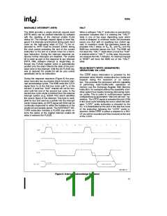
 INTEL [ INTEL ]