®
MOBILE PENTIUM PROCESSOR WITH MMX™ TECHNOLOGY
4.4.1.
BUFFER MODEL PARAMETERS
values; if it is operating as a driver, use all of the
data parameters.
This section gives the parameters for each input,
output and bidirectional buffers.
Please refer to Table 19 for the groupings of the
buffers.
The input, output and bidirectional buffer values of
the processor are listed in Table 20. These tables
contain listings for all three types, do not get them
confused during simulation. When a bidirectional
pin is operating as an input, use the CIN, CP and LP
The input, output and bi-directional buffer’s values
are listed below. These tables contain listings for all
three types. When a bi-directional pin is operating
as an input, just use the CIN, CP and LP values, if it
is operating as a driver use all the data parameters.
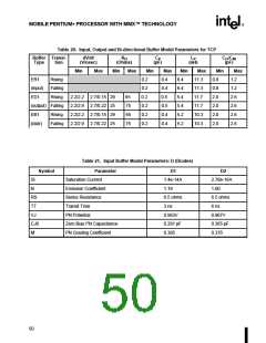
Table 19. TCP Signal to Buffer Type
Driver Buffer Receiver Buffer
Signals
Type
Type
Type
A20M#, AHOLD, BF, BOFF#, BRDY#, BUSCHK#, EADS#,
EWBE#, FLUSH#, HOLD, IGNNE#, INIT, INTR, INV,
KEN#, NA#, NMI, PEN#, PICCLK, R/S#, RESET, SMI#,
STPCLK#, TCK, TDI, TMS, TRST#, WB/WT#
I
ER1
APCHK#, BE[7:5]#, BP[3:2], BREQ, FERR#, IERR#, PCD,
PCHK#, PM0/BP0, PM1/BP1, PRDY, PWT, SMIACT#,
TDO
O
ED1
EB1
A[31: 3], AP, BE[4:0]#, CACHE#, D/C#, D[63:0], DP[8:0],
HLDA, LOCK#, M/IO#, SCYC, ADS#, HITM#, HIT#, W/R#,
PICD0, PICD1
I/O
EB1
49

 INTEL [ INTEL ]