Electrical Specifications
3.
4.
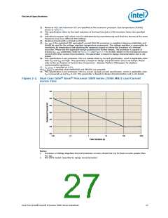
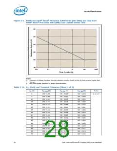
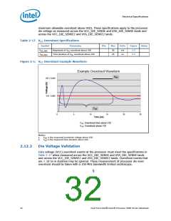
Refer to Table 2-11 for processor VCC information.
The load lines specify voltage limits at the die measured at the VCC_DIE_SENSE and VSS_DIE_SENSE
lands and at the VCC_DIE_SENSE2 and VSS_DIE_SENSE2 lands. Voltage regulation feedback for voltage
regulator circuits must also be taken from processor VCC_DIE_SENSE and VSS_DIE_SENSE lands and
VCC_DIE_SENSE2 and VSS_DIE_SENSE2 lands. Please refer to the appropriate platform design guide for
details on VR implementation.
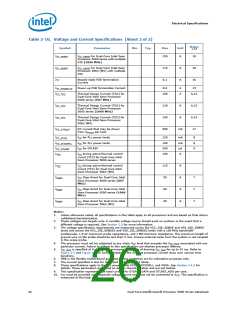
Table 2-12. BSEL[2:0], VID[5:0] Signal Group DC Specifications
1
Symbol
Parameter
Min
Max
Units
Notes
R
BSEL[2:0], VID[5:0]
Buffer On Resistance
N/A
120
2
ON
Ω
I
I
Output Low Current
Output High Current
Voltage Tolerance
N/A
N/A
2.4
460
mA
µA
V
2, 3
2, 3
4
OL
OH
V
0.95 * V
1.05 * V
TT
TOL
TT
Notes:
1.
2.
3.
4.
Unless otherwise noted, all specifications in this table apply to all processor frequencies.
These parameters are based on design characterization and are not tested.
I
is measured at 0.10*V , I
is measured at 0.90*V .
OL
TT OH TT
Please refer to the appropriate platform design guide for implementation details.
Table 2-13. AGTL+ Signal Group DC Specifications
1
Symbol
Parameter
Min
Max
Unit
Notes
V
V
V
Input Low Voltage
Input High Voltage
Output High Voltage
Output Low Current
0.0
GTLREF - (0.10 * V
)
TT
V
V
2
3, 4
4
IL
IH
GTLREF + (0.10 * V
)
V
V
TT
TT
TT
0.90 * V
N/A
V
OH
OL
TT
I
V
/
mA
4
TT
(0.50 * R
+ R
)
ON_MIN
TT_MIN
I
I
Input Leakage Current
Output Leakage Current
Buffer On Resistance
N/A
N/A
7
± 200
± 200
11
µA
µA
5, 6
5, 6
7
LI
LO
R
ON
Ω
Notes:
1.
2.
3.
4.
Unless otherwise noted, all specifications in this table apply to all processor frequencies.
V
V
V
is defined as the voltage range at a receiving agent that will be interpreted as an electrical low value.
is defined as the voltage range at a receiving agent that will be interpreted as an electrical high value.
IL
IH
IH
and V
may experience excursions above V . However, input signal drivers must comply with the
OH
TT
signal quality specifications in Section 3.
Leakage to V with land held at V .
5.
6.
7.
SS
TT
Leakage to V with land held at 300 mV.
TT
This parameter is based on design characterization and is not tested
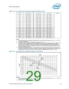
Table 2-14. PWRGOOD Input and TAP Signal Group DC Specifications (Sheet 1 of 2)
1,
Notes
2
Symbol
Parameter
Min
Max
Unit
V
V
Input Hysteresis
120
396
mV
V
3
HYS
t+
PWRGOOD Input Low to
High Threshold Voltage
0.5 * (V + V
+
0.5 * (V + V
HYS_MAX
+
)
TT
HYS_MIN
TT
0.24)
0.24)
TAP Input Low to High
Threshold Voltage
0.5 * (V + V
)
0.5 * (V + V
V
V
V
V
TT
HYS_MIN
TT
HYS_MAX
TT
PWRGOOD Input High to
Low Threshold Voltage
0.4 * V
0.6 * V
0.5 * (V - V
TT
V
V
t-
TAP Input High to Low
Threshold Voltage
0.5 * (V -V
TT
)
)
HYS_MIN
HYS_MAX
TT
Output High Voltage
N/A
V
4
OH
TT
30
Dual-Core Intel® Xeon® Processor 5000 Series Datasheet

 INTEL [ INTEL ]