Electrical Specifications
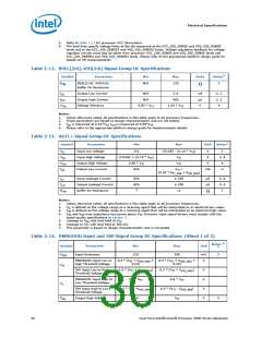
Table 2-14. PWRGOOD Input and TAP Signal Group DC Specifications (Sheet 2 of 2)
1,
Notes
2
Symbol
Parameter
Min
Max
Unit
I
I
Input Leakage Current
Output Leakage Current
Buffer On Resistance
N/A
N/A
7
± 200
± 200
11
µA
µA
LI
LO
R
5
ON
Ω
Notes:
1.
2.
3.
Unless otherwise noted, all specifications in this table apply to all processor frequencies.
All outputs are open drain.
V
represents the amount of hysteresis, nominally centered about 0.5 * V for all PWRGOOD and TAP
HYS
TT
inputs.
4.
5.
PWRGOOD input and the TAP signal group must meet system signal quality specification in Section 3.
The maximum output current is based on maximum current handling capability of the buffer and is not
specified into the test load.
Table 2-15. GTL+ Asynchronous and AGTL+ Asynchronous Signal Group
DC Specifications
1
Symbol
Parameter
Min
Max
(0.5 * V ) - (0.10 * V )
TT
Unit Notes
V
Input Low Voltage
0.0
V
V
3, 11
IL
TT
4, 5, 7,
11
V
Input High Voltage
Output High Voltage
Output Low Current
Input Leakage Current
(0.5 * V ) + (0.10 * V
)
V
V
IH
TT
TT
TT
TT
V
0.90*V
-
V
2, 5, 7
OH
OL
TT
V
/
TT
I
I
A
8
9
[(0.50*R
)+(R
)]
ON_MIN
TT_MIN
I
N/A
N/A
± 200
µA
µA
LI
Output Leakage
Current
± 200
11
10
LO
R
Buffer On Resistance
7
6
Ω
ON
Notes:
1.Unless otherwise noted, all specifications in this table apply to all processor frequencies.
2.All outputs are open drain.
3.V is defined as the voltage range at a receiving agent that will be interpreted as a logical low value.
IL
4.V is defined as the voltage range at a receiving agent that will be interpreted as a logical high value.
IH
IH
5.V and V
may experience excursions above V . However, input signal drivers must comply with the signal
OH
TT
quality specifications in Section 3.
6.Refer to the processor HSPICE* I/O Buffer Models for I/V characteristics.
7.The V referred to in these specifications refers to instantaneous V .
TT
TT
8.The maximum output current is based on maximum current handling capability of the buffer and is not
specified into the test load.
9.Leakage to V with land held at V .
SS
TT
10.Leakage to V with land held at 300 mV.
TT
11.LINT0/INTR and LINT1/NMI use GTLREF_ADD as a reference voltage. For these two signals V
=
IH
GTLREF_ADD + (0.10 * V ) and V = GTLREF_ADD - (0.10 * V ).
TT
IL
TT
Table 2-16. VTTPWRGD DC Specifications
Symbol
Parameter
Min
Max
Unit
V
V
Input Low Voltage
Input High Voltage
0.0
0.30
V
V
IL
0.90
V
TT
IH
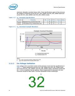
2.12.1
V
Overshoot Specification
CC
The Dual-Core Intel Xeon Processor 5000 series can tolerate short transient overshoot
events where VCC exceeds the VID voltage when transitioning from a high-to-low
current load condition. This overshoot cannot exceed VID + VOS_MAX (VOS_MAX is the
Dual-Core Intel® Xeon® Processor 5000 Series Datasheet
31

 INTEL [ INTEL ]