Processor Configuration Registers
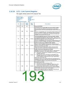
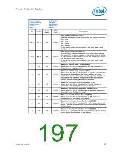
B/D/F/Type:
Address Offset:
Reset Value:
Access:
0/6/0/PCI
B0–B1h
0000h
RO, RW, RW-V
16 bits
Size:
BIOS Optimal Default
00h
Reset
Value
RST/
PWR
Bit
Access
Description
Common Clock Configuration (CCC)
0 = This component and the component at the opposite end of
this Link are operating with asynchronous reference clock.
1 = This component and the component at the opposite end of
this Link are operating with a distributed common reference
clock.
6
RW
0b
Uncore
The state of this bit affects the L0s Exit Latency reported in
LCAP[14:12] and the N_FTS value advertised during link training.
See L0SLAT at offset 22Ch.
Retrain Link (RL)
0 = Normal operation.
1 = Full Link retraining is initiated by directing the Physical Layer
LTSSM from L0, L0s, or
5
RW-V
0b
Uncore
L1 states to the Recovery state.
This bit always returns 0 when read. This bit is cleared
automatically (no need to write a 0).
Link Disable (LD):
0 = Normal operation
1 = Link is disabled. Forces the LTSSM to transition to the
Disabled state (using Recovery) from L0, L0s, or L1 states.
Link retraining happens automatically on 0 to 1 transition,
just like when coming out of reset.
4
RW
0b
Uncore
Writes to this bit are immediately reflected in the value read from
the bit, regardless of actual Link state.
After clearing this bit, software must honor timing requirements
defined in the PCIe Specification, Section 6.6.1 with respect to
the first Configuration Read following a Conventional Reset.
Read Completion Boundary (RCB)
Hardwired to 0 to indicate 64 byte.
3
2
RO
RO
0b
0h
Uncore
Uncore
Reserved (RSVD)
Active State PM (ASPM):
This field controls the level of ASPM (Active State Power
Management) supported on the given PCI Express Link.
1:0
RW
00b
194
Datasheet, Volume 2

 INTEL [ INTEL ]