Processor Configuration Registers
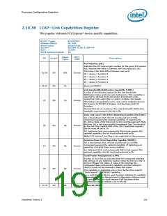
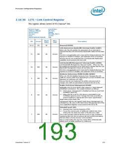
B/D/F/Type:
Address Offset:
Reset Value:
Access:
0/6/0/PCI
AC–AFh
0521CC42h
RO, RW-O, RO-V, RW-OV
32 bits
Size:
BIOS Optimal Default
0h
Reset
Value
RST/
PWR
Bit
Access
Description
L0s Exit Latency (L0SELAT)
This field indicates the length of time this Port requires to
complete the transition from L0s to L0.
000 = Less than 64 ns
001 = 64 ns to less than 128 ns
010 = 128 ns to less than 256 ns
011 = 256 ns to less than 512 ns
100 = 512 ns to less than 1 us
101 = 1 us to less than 2 us
110 = 2 us – 4 us
14:12
RO-V
100b
Uncore
111 = More than 4 us
The actual value of this field depends on the common Clock
Configuration bit (LCTL[6]) and the Common and Non-Common
clock L0s Exit Latency values in L0SLAT (Offset 22Ch)
Active State Link PM Support (ASLPMS)
Root port supports ASPM L0s and L1.
11:10
RW-O
11b
Uncore
Uncore
Max Link Width (MLW):
This field indicates the maximum number of lanes supported for
this link.
9:4
3:0
RW-OV
RO
04h
0h
Reserved (RSVD)
192
Datasheet, Volume 2

 INTEL [ INTEL ]