Processor Configuration Registers
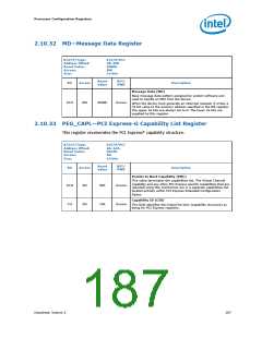
2.10.32 MD—Message Data Register
B/D/F/Type:
Address Offset:
Reset Value:
Access:
0/6/0/PCI
98–99h
0000h
RW
16 bits
Size:
Reset
Value
RST/
PWR
Bit
Access
Description
Message Data (MD)
Base message data pattern assigned by system software and
used to handle an MSI from the device.
When the device must generate an interrupt request, it writes a
32-bit value to the memory address specified in the MA register.
The upper 16 bits are always set to 0. The lower 16 bits are
supplied by this register.
15:0
RW
0000h
Uncore
2.10.33 PEG_CAPL—PCI Express-G Capability List Register
This register enumerates the PCI Express* capability structure.
B/D/F/Type:
Address Offset:
Reset Value:
Access:
0/6/0/PCI
A0–A1h
0010h
RO
Size:
16 bits
Reset
Value
RST/
PWR
Bit
Access
Description
Pointer to Next Capability (PNC)
This value terminates the capabilities list. The Virtual Channel
capability and any other PCI Express specific capabilities that are
reported using this mechanism are in a separate capabilities list
located entirely within PCI Express Extended Configuration
Space.
15:8
RO
00h
10h
Uncore
Uncore
Capability ID (CID)
This field identifies this linked list item (capability structure) as
being for PCI Express registers.
7:0
RO
Datasheet, Volume 2
187

 INTEL [ INTEL ]