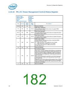
Processor Configuration Registers
B/D/F/Type:
Address Offset:
Reset Value:
Access:
0/6/0/PCI
92–93h
0000h
RO, RW
16 bits
00h
Size:
BIOS Optimal Default
Reset
Value
RST/
PWR
Bit
Access
Description
Multiple Message Enable (MME)
System software programs this field to indicate the actual
number of messages allocated to this device. This number will be
equal to or less than the number actually requested.
6:4
RW
000b
Uncore
The encoding is the same as for the MMC field below.
Multiple Message Capable (MMC)
System software reads this field to determine the number of
messages being requested by this device.
000 = 1
All of the following are reserved in this implementation:
001 = 2
010 = 4
3:1
RO
000b
Uncore
011 = 8
100 = 16
101 = 32
110 = Reserved
111 = Reserved
MSI Enable (MSIEN)
This bit controls the ability of this device to generate MSIs.
0 = MSI will not be generated.
1 = MSI will be generated when we receive PME messages. INTA
will not be generated and INTA Status (PCISTS1[3]) will not
be set.
0
RW
0b
Uncore
2.10.31 MA—Message Address Register
B/D/F/Type:
Address Offset:
Reset Value:
Access:
0/6/0/PCI
94-97h
00000000h
RW, RO
32 bits
Size:
Reset
Value
RST/
PWR
Bit
Access
Description
Message Address (MA)
Used by system software to assign an MSI address to the device.
The device handles an MSI by writing the padded contents of the
MD register to this address.
31:2
RW
00000000h
Uncore
Uncore
Force DWord Align (FDWA)
Hardwired to 0 so that addresses assigned by system software
are always aligned on a DWord address boundary.
1:0
RO
00b
186
Datasheet, Volume 2

 INTEL [ INTEL ]