Electrical Specifications
probe capacitance, and 1 MΩ minimum impedance. The maximum length of ground wire on the probe
should be less than 5 mm. Ensure external noise from the system is not coupled in the scope probe.
The V voltage specification requirements are measured across vias on the platform for the
7.
CACHE
VCACHESENSE and VSSCACHESENSE pins close to the socket with a 100 MHz bandwidth oscilloscope, 1.5
pF maximum probe capacitance, and 1 MΩ minimum impedance. The maximum length of ground wire on
the probe should be less than 5 mm. Ensure external noise from the system is not coupled in the scope
probe.
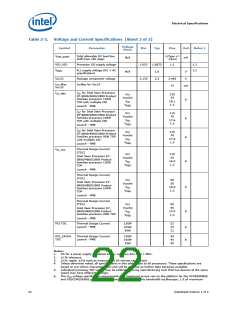
Table 2-6.
Processor Vcc Static and Transient Tolerance
I
(A)
Vcc
(V)
Vcc
(V)
Vcc (V)
_Min
Notes
CC
_Max
_Typ
0
VID - 0.000
VID - 0.004
VID - 0.008
VID - 0.012
VID - 0.016
VID - 0.020
VID - 0.024
VID - 0.028
VID - 0.032
VID - 0.036
VID - 0.040
VID - 0.044
VID - 0.048
VID - 0.052
VID - 0.056
VID - 0.060
VID - 0.064
VID - 0.068
VID - 0.072
VID - 0.076
VID - 0.080
VID - 0.084
VID - 0.088
VID - 0.092
VID - 0.096
VID - 0.100
VID - 0.104
VID - 0.108
VID - 0.112
VID - 0.116
VID - 0.120
VID - 0.015
VID - 0.019
VID - 0.023
VID - 0.027
VID - 0.031
VID - 0.035
VID - 0.039
VID - 0.043
VID - 0.047
VID - 0.051
VID - 0.055
VID - 0.059
VID - 0.063
VID - 0.067
VID - 0.071
VID - 0.075
VID - 0.079
VID - 0.083
VID - 0.087
VID - 0.091
VID - 0.095
VID - 0.099
VID - 0.103
VID - 0.107
VID - 0.111
VID - 0.115
VID - 0.119
VID - 0.123
VID - 0.127
VID - 0.131
VID - 0.135
VID - 0.030
VID - 0.034
VID - 0.038
VID - 0.042
VID - 0.046
VID - 0.050
VID - 0.054
VID - 0.058
VID - 0.062
VID - 0.066
VID - 0.070
VID - 0.074
VID - 0.078
VID - 0.082
VID - 0.086
VID - 0.090
VID - 0.094
VID - 0.098
VID - 0.102
VID - 0.106
VID - 0.110
VID - 0.114
VID - 0.118
VID - 0.122
VID - 0.126
VID - 0.130
VID - 0.134
VID - 0.138
VID - 0.142
VID - 0.146
VID - 0.150
-
5
10
15
20
25
30
35
40
45
50
55
60
65
70
75
80
85
90
95
100
105
110
115
120
125
130
135
140
145
150
Notes:
1.
The Vcc
and Vcc
loadlines represent static and transient limits. Please see Table 2-8 and
_MIN
_MAX
Figure 2-3 for Vcc overshoot specifications.
2.
The loadlines specify voltage limits at the die. Die Vcc voltage is available at the Vcoresense and
Vsscoresense lands and should be measured there. Voltage regulation feedback for voltage regulator
circuits must be taken from the processor VCORESENSE and VSSCORESENSE lands. Voltage regulation
feedback for voltage regulator circuits must also be taken from processor VCCCORESENSE and
VSSCORESENSE lands. Refer to the Voltage Regulator Module (VRM) and Enterprise Voltage Regulator
Down (EVRD) 11.1 Design Guidelines for socket load line guidelines and VR implementation
Datasheet Volume 1 of 2
23

 INTEL [ INTEL ]