Electrical Specifications
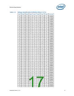
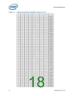
Table 2-3.
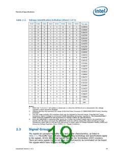
Signal Groups (Sheet 2 of 2)
1
Signal Group
VID
Type
Signals
Single ended
Single ended
CMOS Output
Open/Ground
VID[7:0], CVID[7:1]
VIO_VID[4:1]
Voltage, and Voltage Regulator
Differential
Power
Power
ISENSE_DN, ISENSE_DP
Single ended
Vcc, VREG, VCACHE, VCACHESENSE,
VCC33,VCORESENSE, VIO, PSI_CACHE_N,PSI_N,
VSSCACHESENSE,VSSCORESENSE,
Debug
Single ended
GTL I/O-OD
MBP[7:0]_N, PRDY_N,PREQ_N
Notes:
1.
See Chapter 5 for signal descriptions.
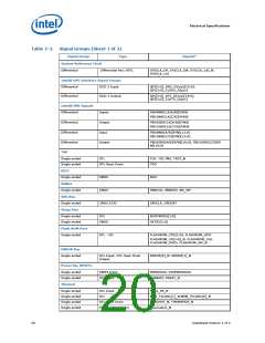
Table 2-4.
Signals with RTT
Signals with RTT
•
•
QPI[3:0]R[P/N]Dat[19:0], QPI[5:4]R[P/N]CLK0, QPI[3:0]T[P/N]Dat[19:0],
QPI[5:4]T[P/N]CLK0
FBD0NBICLK[A/B][P/N]0, FBD1NBICLK[C/D][P/N]0, FBD0SBOCLK[A/B][P/N]0,
FBD1SBOCLK[C/D][P/N]0, FBD0NBI[A/B][P/N][12:0], FBD1NBI[C/D][P/
N][12:0], FBD0SBO[A/B][P/N][9:0], FBD1SBO[C/D][P/N][9:0].
2.4
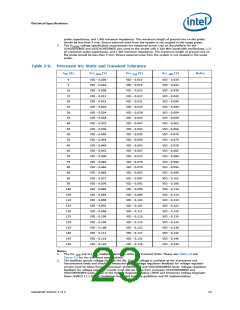
Processor DC Specifications
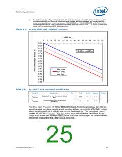
Voltage and current specifications are detailed in Table 2-5. For platform planning refer
to Table 2-6, which provides Vcc static and transient tolerances.
Differential SYSCLK specifications are found in Table 2-26. Control Sideband and Test
Access Port (TAP) are listed in Table 2-24.
Table 2-5 through Table 2-24 list the DC specifications for the processor and are valid
only while meeting specifications for case temperature (TCASE as specified in Chapter 6,
“Thermal Specifications”), clock frequency, and input voltages. Care should be taken to
read all notes associated with each parameter.
Table 2-5.
Voltage and Current Specifications (Sheet 1 of 2)
Voltage
Symbol
Parameter
Min
Typ
Max
Unit
V
Notes 1
4,5
Plane
VID
VCore VID range
for processor core
Launch - FMB
Vcc Load Line
VCache VID range
Vcc for cache
N/A
0.60
1.35
Vcc
V
4,5,6
CC
See Table 2-6
V
Vcc LL
CVID
0.8
mΩ
V
0.7
1.35
4,5
V
V
V
See Table 2-7
1.4
V
4,5,7
CACHE
CACHE
LL
V
Load Line
mΩ
CACHE
Vcc VID step size during a
transition
VID_STEP
N/A
± ±6.25
mV
Datasheet Volume 1 of 2
21

 INTEL [ INTEL ]