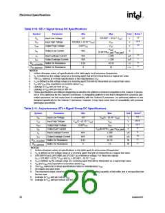
Electrical Specifications
2.13
GTL+ FSB Specifications
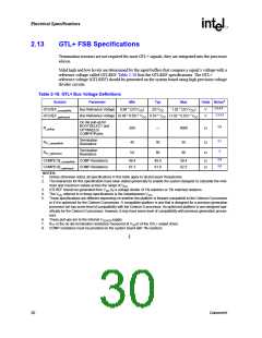
Termination resistors are not required for most GTL+ signals; they are integrated into the processor
silicon.
Valid high and low levels are determined by the input buffers that compare a signal’s voltage with a
reference voltage called GTLREF. Table 2-18 lists the GTLREF specifications. The GTL+
reference voltage (GTLREF) should be generated on the system board using high precision voltage
divider circuits.
Table 2-18. GTL+ Bus Voltage Definitions
1
Symbol
Parameter
Min
Typ
2/3 V
Max
Units Notes
2,3,4,5
GTLREF
Bus Reference Voltage
0.98 * (2/3 V
)
1.02 * (2/3 V
CC
)
V
_compatible
CC
CC
2,3,4,5
5,6
GTLREF
Bus Reference Voltage (0.98 * 0.63) * V
0.63 * V
(1.02 * 0.63) * V
V
_optimized
CC
CC
CC
On die pull-up for
BOOTSELECT and
500
R
—
5000
Ω
_pullup
OPTIMIZED/
COMPAT# pins
Termination
45
5,7
5
RTT_compatible
RTT_optimized
50
60
55
66
Ω
Ω
Resistance
Termination
54
Resistance
5,8
5,8
COMP[1:0]
COMP[1:0]
NOTES:
COMP Resistance
COMP Resistance
49.4
61.3
49.9
61.9
50.4
62.5
Ω
Ω
_compatible
_optimized
1. Unless otherwise noted, all specifications in this table apply to all processor frequencies.
2. The tolerances for this specification have been stated generically to enable the system designer to calculate the mini-
mum and maximum values across the range of V
.
CC
3. GTLREF should be generated from V by a voltage divider of 1% resistors or 1% matched resistors.
CC
4. The V referred to in these specifications is the instantaneous V
.
CC
CC
5. These specifications are different depending on whether the platform is forward compatible to the Celeron D processor
or if it is optimized for the Celeron D processor. A compatible platform is one that is designed for a previous generation
processor but has some level of compatibility with the Celeron D processor. An optimized platform is one designed spe-
cifically for the Celeron D processor; however, it may have some level of compatibility with previous generation proces-
sors.
6. These pull-ups are to the internal V
supply.
CCVID
7.
R
is the on-die termination resistance measured at V /2 of the GTL+ output driver.
TT CC
8. COMP resistance must be provided on the system board with 1% resistors.
§
30
Datasheet

 INTEL [ INTEL ]