Functional Description
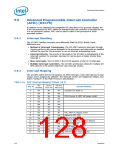
Table 5-16. APIC Interrupt Mapping1 (Sheet 2 of 2)
Via
SERIRQ
Direct
from Pin
Via PCI
Message
IRQ #
Internal Modules
16
17
18
19
20
21
22
23
PIRQA#
PIRQB#
PIRQC#
PIRQD#
N/A
PIRQA#
PIRQB#
PIRQC#
PIRQD#
PIRQE#4
PIRQF#4
PIRQG#4
PIRQH#4
Internal devices are routable; see
Section 10.1.54 though Section 10.1.60.
Yes
Yes
Option for SCI, TCO, HPET #0,1,2, 3. Other
internal devices are routable; see
Section 10.1.54 through Section 10.1.60.
N/A
N/A
N/A
NOTES:
1.
2.
3.
4.
When programming the polarity of internal interrupt sources on the APIC, interrupts 0
through 15 receive active-high internal interrupt sources, while interrupts 16 through 23
receive active-low internal interrupt sources.
If IRQ 11 is used for HPET #2, software should ensure IRQ 11 is not shared with any other
devices to ensure the proper operation of HPET #2. ICH10 hardware does not prevent
sharing of IRQ 11.
If IRQ 12 is used for HPET #3, software should ensure IRQ 12 is not shared with any other
devices to ensure the proper operation of HPET #3. ICH10 hardware does not prevent
sharing of IRQ 12.
PIRQ[E:H] are Multiplexed with GPIO pins. Interrupts PIRQ[E:H] will not be exposed if they
are configured as GPIOs.
5.9.3
5.9.4
PCI / PCI Express* Message-Based Interrupts
When external devices through PCI / PCI Express wish to generate an interrupt, they
will send the message defined in the PCI Express* Base Specification, Revision 1.0a for
generating INTA# - INTD#. These will be translated internal assertions/de-assertions of
INTA# – INTD#.
Front Side Bus Interrupt Delivery
For processors that support Front Side Bus (FSB) interrupt delivery, the ICH10 requires
that the I/O APIC deliver interrupt messages to the processor in a parallel manner,
rather than using the I/O APIC serial scheme.
This is done by the ICH10 writing (via DMI) to a memory location that is snooped by
the processor(s). The processor(s) snoop the cycle to know which interrupt goes active.
The following sequence is used:
1. When the ICH10 detects an interrupt event (active edge for edge-triggered mode
or a change for level-triggered mode), it sets or resets the internal IRR bit
associated with that interrupt.
2. Internally, the ICH10 requests to use the bus in a way that automatically flushes
upstream buffers. This can be internally implemented similar to a DMA device
request.
3. The ICH10 then delivers the message by performing a write cycle to the
appropriate address with the appropriate data. The address and data formats are
described below in Section 5.9.4.4.
Note:
FSB Interrupt Delivery compatibility with processor clock control depends on the
processor, not the ICH10.
Datasheet
129

 INTEL [ INTEL ]