Introduction
1
Introduction
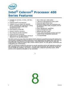
The Intel® Celeron® processor 400 series is a desktop processor that combines the
performance of the previous generation of Desktop products with the power efficiencies
of a low-power microarchitecture to enable smaller, quieter systems. Intel Celeron
Processor 400 is a 64-bit processor that maintain compatibility with IA-32 software.
The Intel Celeron processor 400 series uses a Flip-Chip Land Grid Array (FC-LGA6)
package technology, and plugs into a 775-land surface mount, Land Grid Array (LGA)
socket, referred to as the LGA775 socket.
Note:
Note:
In this document the Intel Celeron processor 400 series will be referred to as "the
processor."
In this document the Intel Celeron processor 400 series refers to the Intel Celeron
processors 420, 430, 440, and 450.
Based on 65 nm process technology, the Intel Celeron processor 400 series is a single-
core processor that features an 800 MHz front side bus (FSB), 1 MB or 512 KB L2
cache, and a thermal design power (TDP) of 35 W. The processor also supports the
Execute Disable Bit and Intel® 64 architecture.
The processor front side bus (FSB) uses a split-transaction, deferred reply protocol like
the Intel® Pentium® 4 processor. The FSB uses Source-Synchronous Transfer (SST) of
address and data to improve performance by transferring data four times per bus clock
(4X data transfer rate, as in AGP 4X). Along with the 4X data bus, the address bus can
deliver addresses two times per bus clock and is referred to as a "double-clocked" or 2X
address bus. Working together, the 4X data bus and 2X address bus provide a data bus
bandwidth of up to 6.4 GB/s.
Intel will enable support components for the processor including heatsink, heatsink
retention mechanism, and socket. Supported platforms may need to be refreshed to
ensure the correct voltage regulation (VRD11) and that PECI support is enabled.
Manufacturability is a high priority; hence, mechanical assembly may be completed
from the top of the baseboard and should not require any special tooling.
The processor includes an address bus power-down capability which removes power
from the address and data signals when the FSB is not in use. This feature is always
enabled on the processor.
1.1
Terminology
A ‘#’ symbol after a signal name refers to an active low signal, indicating a signal is in
the active state when driven to a low level. For example, when RESET# is low, a reset
has been requested. Conversely, when NMI is high, a nonmaskable interrupt has
occurred. In the case of signals where the name does not imply an active state but
describes part of a binary sequence (such as address or data), the ‘#’ symbol implies
that the signal is inverted. For example, D[3:0] = ‘HLHL’ refers to a hex ‘A’, and
D[3:0]# = ‘LHLH’ also refers to a hex ‘A’ (H= High logic level, L= Low logic level).
Front Side Bus” refers to the interface between the processor and system core logic
(a.k.a. the chipset components). The FSB is a multiprocessing interface to processors,
memory, and I/O.
Datasheet
9

 INTEL [ INTEL ]