Pin Listing and Signal Definitions
Table 37. Signal Description (Page 4 of 8)
Name
Type
Description
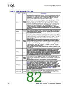
DPSLP# when asserted on the platform causes the processor to transition from the
Sleep State to the Deep Sleep state. In order to return to the Sleep State, DPSLP#
must be deasserted and BCLK[1:0] must be running.
DPSLP#
Input
DRDY# (Data Ready) is asserted by the data driver on each data transfer,
Input/ indicating valid data on the data bus. In a multi-common clock data transfer, DRDY#
Output may be deasserted to insert idle clocks. This signal must connect the appropriate
pins of all processor system bus agents.
DRDY#
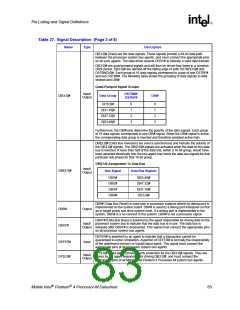
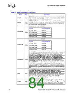
Data strobe used to latch in D[63:0]#.
Signals
Associated Strobe
D[15:0]#, DBI0#
D[31:16]#, DBI1#
D[47:32]#, DBI2#
D[63:48]#, DBI3#
DSTBN0#
DSTBN1#
DSTBN2#
DSTBN3#
Input/
Output
DSTBN[3:0]#
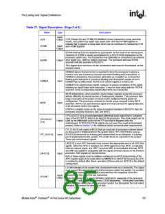
Data strobe used to latch in D[63:0]#.
Signals
Associated Strobe
D[15:0]#, DBI0#
D[31:16]#, DBI1#
D[47:32]#, DBI2#
D[63:48]#, DBI3#
DSTBP0#
DSTBP1#
DSTBP2#
DSTBP3#
Input/
Output
DSTBP[3:0]#
FERR#/PBE# (floating point error/pending break event) is a multiplexed signal and
its meaning is qualified by STPCLK#. When STPCLK# is not asserted, FERR#/
PBE# indicates a floating-point error and will be asserted when the processor
detects an unmasked floating-point error. When STPCLK# is not asserted, FERR#/
PBE# is similar to the ERROR# signal on the INTEL 387 coprocessor, and is
included for compatibility with systems using MS-DOS*-type floating-point error
reporting. When STPCLK# is asserted, an assertion of FERR#/PBE# indicates that
FERR#/PBE# Output the processor has a pending break event waiting for service. The assertion of
FERR#/PBE# indicates that the processor should be returned to the Normal state.
When FERR#/PBE# is asserted, indicating a break event, it will remain asserted
until STPCLK# is deasserted. For additional information on the pending break
event functionality, including the identification of support of the feature and enable/
disable information, refer to volume 3 of the Intel Architecture Software Developer's
Manual and the Intel Processor Identification and the CPUID Instruction application
note.
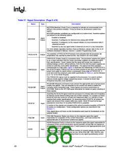
The GHI# signal controls the selection of the operating mode bus ratio and voltage
in the Mobile Intel Pentium 4 Processor-M. On the Mobile Intel Pentium 4
Processor-M featuring Enhanced Intel SpeedStep technology, this signal is latched
on entry to Sleep state and is observed during the Deep Sleep state. GHI#
GHI#
Input
Input
determines which of two performance states is selected for operation. This signal is
ignored when the processor is not in the Deep Sleep state. This signal should be
driven with an Open-drain driver. Refer to the Mobile Intel Pentium
Processor-M and Intel 845MP/845MZ Chipset Platform Design Guide for
4
termination and connection guidelines.
GTLREF determines the signal reference level for AGTL+ input pins. GTLREF
should be set at 2/3 VCC. GTLREF is used by the AGTL+ receivers to determine if a
GTLREF
signal is a logical 0 or logical 1. Refer to the Mobile Intel Pentium 4 Processor-M
and Intel 845MP/845MZ Chipset Platform Design Guide for more information.
84
Mobile Intel Pentium 4 Processor-M Datasheet

 INTEL [ INTEL ]