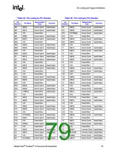
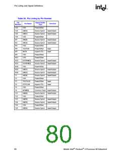
Pin Listing and Signal Definitions
Table 37. Signal Description (Page 3 of 8)
Name
Type
Description
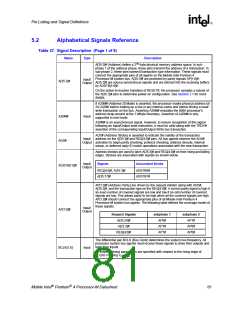
D[63:0]# (Data) are the data signals. These signals provide a 64-bit data path
between the processor system bus agents, and must connect the appropriate pins
on all such agents. The data driver asserts DRDY# to indicate a valid data transfer.
D[63:0]# are quad-pumped signals and will thus be driven four times in a common
clock period. D[63:0]# are latched off the falling edge of both DSTBP[3:0]# and
DSTBN[3:0]#. Each group of 16 data signals correspond to a pair of one DSTBP#
and one DSTBN#. The following table shows the grouping of data signals to data
strobes and DBI#.
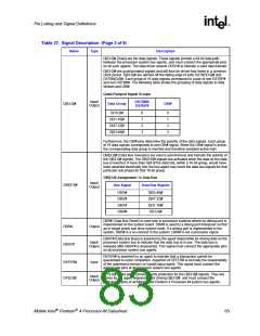
Quad-Pumped Signal Groups
DSTBN#/
Input/
Output
D[63:0]#
Data Group
DBI#
DSTBP#
D[15:0]#
D[31:16]#
D[47:32]#
D[63:48]#
0
1
2
3
0
1
2
3
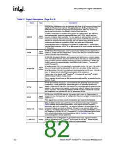
Furthermore, the DBI# pins determine the polarity of the data signals. Each group
of 16 data signals corresponds to one DBI# signal. When the DBI# signal is active,
the corresponding data group is inverted and therefore sampled active high.
DBI[3:0]# (Data Bus Inversion) are source synchronous and indicate the polarity of
the D[63:0]# signals. The DBI[3:0]# signals are activated when the data on the data
bus is inverted. If more than half of the data bits, within a 16-bit group, would have
been asserted electrically low, the bus agent may invert the data bus signals for that
particular sub-phase for that 16-bit group.
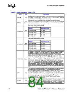
DBI[3:0] Assignment To Data Bus
Input/
Output
DBI[3:0]#
Bus Signal
Data Bus Signals
DBI3#
DBI2#
DBI1#
DBI0#
D[63:48]#
D[47:32]#
D[31:16]#
D[15:0]#
DBR# (Data Bus Reset) is used only in processor systems where no debug port is
implemented on the system board. DBR# is used by a debug port interposer so that
an in-target probe can drive system reset. If a debug port is implemented in the
system, DBR# is a no connect in the system. DBR# is not a processor signal.
DBR#
Output
DBSY# (Data Bus Busy) is asserted by the agent responsible for driving data on the
Input/ processor system bus to indicate that the data bus is in use. The data bus is
Output released after DBSY# is deasserted. This signal must connect the appropriate pins
on all processor system bus agents.
DBSY#
DEFER# is asserted by an agent to indicate that a transaction cannot be
guaranteed in-order completion. Assertion of DEFER# is normally the responsibility
of the addressed memory or Input/Output agent. This signal must connect the
appropriate pins of all processor system bus agents.
DEFER#
DP[3:0]#
Input
DP[3:0]# (Data parity) provide parity protection for the D[63:0]# signals. They are
Input/
driven by the agent responsible for driving D[63:0]#, and must connect the
Output
appropriate pins of all Mobile Intel Pentium 4 Processor-M system bus agents.
Mobile Intel Pentium 4 Processor-M Datasheet
83

 INTEL [ INTEL ]