欢迎访问ic37.com |
会员登录 免费注册
发布采购

21150-AB 参数 Datasheet PDF下载

21150-AB图片预览
型号: 21150-AB
PDF下载: 下载PDF文件 查看货源
内容描述: [PCI Bus Controller, CMOS, PQFP208, PLASTIC, QFP-208]
分类和应用: 时钟PC外围集成电路
文件页数/大小: 164 页 / 811 K
品牌: INTEL [ INTEL ]
 浏览型号21150-AB的Datasheet PDF文件第22页浏览型号21150-AB的Datasheet PDF文件第23页浏览型号21150-AB的Datasheet PDF文件第24页浏览型号21150-AB的Datasheet PDF文件第25页浏览型号21150-AB的Datasheet PDF文件第27页浏览型号21150-AB的Datasheet PDF文件第28页浏览型号21150-AB的Datasheet PDF文件第29页浏览型号21150-AB的Datasheet PDF文件第30页  
21150  
3.0  
Pin Assignments  
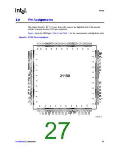
This chapter describes the 21150 pins. It provides numeric and alphabetic lists of the pins and  
includes a diagram showing 21150 pin assignment.  
Figure 5 shows the 21150 pins. Table 13 and Table 14 list the pins in numeric and alphabetic order.  
Figure 5. 21150 Pin Assignment  
vdd  
vss  
vdd  
req_l<1>  
req_l<2>  
req_l<3>  
req_l<4>  
req_l<5>  
req_l<6>  
req_l<7>  
req_l<8>  
gnt_l<0>  
gnt_l<1>  
vss  
gnt_l<2>  
gnt_l<3>  
gnt_l<4>  
gnt_l<5>  
gnt_l<6>  
gnt_l<7>  
gnt_l<8>  
vss  
155  
150  
145  
140  
135  
130  
125  
120  
115  
110  
105  
s_ad<10>  
s_m66ena  
s_ad<9>  
vdd  
s_ad<8>  
s_cbe_l<0>  
vss  
s_ad<7>  
s_ad<6>  
vdd  
s_ad<5>  
s_ad<4>  
vss  
s_ad<3>  
s_ad<2>  
vdd  
s_ad<1>  
s_ad<0>  
vss  
s_vio  
trst_l  
tck  
tms  
vdd  
tdo  
tdi  
nc  
5
10  
15  
20  
25  
30  
35  
40  
45  
50  
s_clk  
s_rst_l  
s_cfn_l  
gpio<3>  
gpio<2>  
vdd  
gpio<1>  
gpio<0>  
clk_o<0>  
clk_o<1>  
vss  
clk_o<2>  
clk_o<3>  
vdd  
clk_o<4>  
clk_o<5>  
vss  
clk_o<6>  
clk_o<7>  
vdd  
clk_o<8>  
clk_o<9>  
p_rst_l  
vss  
21150  
nc  
msk_in  
config66  
p_vio  
vss  
p_ad<0>  
p_ad<1>  
vdd  
p_ad<2>  
p_ad<3>  
vss  
p_ad<4>  
p_ad<5>  
vdd  
p_ad<6>  
p_ad<7>  
vss  
p_cbe_l<0>  
p_ad<8>  
vdd  
p_ad<9>  
vss  
p_clk  
p_gnt_l  
p_req_l  
vss  
p_ad<31>  
p_ad<30>  
vdd  
vss  
vdd  
LJ-04737.AI5  
Preliminary Datasheet  
19  
 
21150  
3.1  
Numeric Pin Assignment  
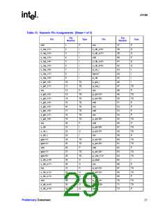
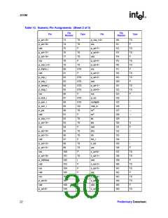
Table 13 lists the 21150 pins in numeric order, showing the name, number, and signal type of each  
pin. Table 12 defines the signal type abbreviations.  
Table 12. Signal Types  
Signal Type  
Description  
I
Standard input only.  
Standard output only.  
Power.  
O
P
TS  
Tristate bidirectional.  
Sustained tristate. Active low signal must be pulled high for one cycle when  
deasserting.  
STS  
OD  
Standard open drain.  
20  
Preliminary Datasheet  
 
21150  
Table 13. Numeric Pin Assignments (Sheet 1 of 3)  
Pin  
Number  
Pin  
Number  
Pin  
Type  
Pin  
Type  
vdd  
1
2
3
4
5
6
7
8
9
P
vss  
37  
P
s_req_l<1>  
s_req_l<2>  
s_req_l<3>  
s_req_l<4>  
s_req_l<5>  
s_req_l<6>  
s_req_l<7>  
s_req_l<8>  
s_gnt_l<0>  
s_gnt_l<1>  
vss  
I
s_clk_o<6>  
s_clk_o<7>  
vdd  
38  
39  
40  
41  
42  
43  
44  
45  
46  
47  
48  
48  
50  
51  
52  
53  
54  
55  
56  
57  
58  
59  
60  
61  
62  
63  
64  
65  
66  
67  
68  
69  
70  
71  
72  
O
I
O
I
P
I
s_clk_o<8>  
s_clk_0<9>  
p_rst_l  
O
I
O
I
I
I
bpcce1  
I
I
p_clk  
I
10  
11  
12  
13  
14  
15  
16  
17  
18  
19  
20  
21  
22  
23  
24  
25  
26  
27  
28  
29  
30  
31  
32  
33  
34  
35  
36  
TS  
TS  
P
p_gnt_l  
p_req_l  
vss  
I
TS  
P
s_gnt_l<2>  
s_gnt_l<3>  
s_gnt_l<4>  
s_gnt_l<5>  
s_gnt_l<6>  
s_gnt_l<7>  
s_gnt_l<8>  
vss  
TS  
TS  
TS  
TS  
TS  
TS  
TS  
P
p_ad<31>  
p_ad<30>  
vdd  
TS  
TS  
P
vss  
P
vdd  
P
vss  
P
p_ad<29>  
vdd  
TS  
P
s_clk  
I
p_ad<28>  
p_ad<27>  
vss  
TS  
TS  
P
s_rst_l  
O
I
s_cfn_l  
gpio<3>  
TS  
TS  
P
p_ad<26>  
p_ad<25>  
vdd  
TS  
TS  
P
gpio<2>  
vdd  
gpio<1>  
TS  
TS  
O
O
P
p_ad<24>  
p_cbe_l<3>  
p_idsel  
vss  
TS  
TS  
I
gpio<0>  
s_clk_o<0>  
s_clk_o<1>  
vss  
P
p_ad<23>  
p_ad<22>  
vdd  
TS  
TS  
P
s_clk_o<2>  
s_clk_o<3>  
vdd  
O
O
P
p_ad<21>  
P_ad<20>  
vss  
TS  
TS  
P
s_clk_o<4>  
s_clk_o<5>  
O
O
Preliminary Datasheet  
21  
21150  
Table 13. Numeric Pin Assignments (Sheet 2 of 3)  
Pin  
Number  
Pin  
Number  
Pin  
Type  
Pin  
p_cbe_l<0>  
Type  
p_ad<19>  
73  
TS  
TS  
P
110  
TS  
P
p_ad<18>  
vdd  
74  
vss  
111  
112  
113  
114  
115  
116  
117  
118  
119  
120  
121  
122  
123  
124  
125  
126  
127  
128  
129  
130  
131  
132  
133  
134  
135  
136  
137  
138  
139  
140  
141  
142  
143  
144  
145  
146  
75  
p_ad<7>  
p_ad<6>  
vdd  
TS  
TS  
P
p_ad<17>  
p_ad<16>  
vss  
76  
TS  
TS  
P
77  
78  
p_ad<5>  
p_ad<4>  
vss  
TS  
TS  
P
p_cbe_l<2>  
p_frame_l  
vdd  
79  
TS  
80  
STS  
P
81  
p_ad<3>  
p_ad<2>  
vdd  
TS  
TS  
P
p_irdy_l  
p_trdy_l  
p_devsel_l  
p_stop_l  
vss  
82  
STS  
STS  
STS  
STS  
P
83  
84  
p_ad<1>  
p_ad<0>  
vss  
TS  
TS  
P
85  
86  
p_lock_l  
p_perr_l  
p_serr_l  
p_par  
87  
STS  
STS  
OD  
TS  
P
p_vio  
I
88  
config66  
msk_in  
nc2  
I
89  
I
90  
I
vdd  
91  
nc2  
p_cbe_l<1>  
p_ad<15>  
vss  
92  
TS  
TS  
P
tdi  
93  
tdo  
O
94  
vdd  
P
p_ad<14>  
p_ad<13>  
vdd  
95  
TS  
TS  
P
tms  
I
96  
tck  
I
97  
trst_l  
I
p_ad<12>  
p_ad<11>  
vss  
98  
TS  
TS  
P
s_vio  
I
99  
vss  
P
100  
101  
102  
103  
104  
105  
106  
107  
108  
109  
s_ad<0>  
s_ad<1>  
vdd  
TS  
TS  
P
p_ad<10>  
p_m66ena  
vdd  
TS  
I
P
s_ad<2>  
s_ad<3>  
vss  
TS  
TS  
P
vss  
P
vdd  
P
vss  
P
s_ad<4>  
s_ad<5>  
vdd  
TS  
TS  
P
p_ad<9>  
vdd  
TS  
P
p_ad<8>  
TS  
s_ad<6>  
TS  
22  
Preliminary Datasheet  
21150  
Table 13. Numeric Pin Assignments (Sheet 3 of 3)  
Pin  
Number  
Pin  
Number  
Pin  
Type  
Pin  
Type  
s_ad<7>  
vss  
147  
TS  
P
vdd  
178  
P
148  
149  
150  
151  
152  
153  
154  
155  
156  
157  
158  
159  
160  
161  
162  
163  
164  
165  
166  
167  
168  
169  
170  
171  
172  
173  
174  
175  
176  
177  
s_frame_l  
179  
180  
181  
182  
183  
184  
185  
186  
187  
188  
189  
190  
191  
192  
193  
194  
195  
196  
197  
198  
199  
200  
201  
202  
203  
204  
205  
206  
207  
208  
STS  
TS  
P
s_cbe_l<0>  
s_ad<8>  
vdd  
TS  
TS  
P
s_cbe_l<2>  
vss  
s_ad<16>  
s_ad<17>  
vdd  
TS  
TS  
P
s_ad<9>  
s_m66ena  
s_ad<10>  
vdd  
TS  
OD  
TS  
P
s_ad<18>  
s_ad<19>  
vss  
TS  
TS  
P
vss  
P
vdd  
P
s_ad<20>  
s_ad<21>  
vdd  
TS  
TS  
P
vss  
P
s_ad<11>  
vss  
TS  
P
s_ad<22>  
s_ad<23>  
vss  
TS  
TS  
P
s_ad<12>  
s_ad<13>  
vdd  
TS  
TS  
P
s_cbe_l<3>  
s_ad<24>  
vdd  
TS  
TS  
P
s_ad<14>  
s_ad<15>  
vss  
TS  
TS  
P
s_ad<25>  
s_ad<26>  
vss  
TS  
TS  
P
s_cbe<1>  
s_par  
TS  
TS  
I
s_serr_l  
vdd  
s_ad<27>  
s_ad<28>  
vdd  
TS  
TS  
P
P
s_perr_l  
s_lock_l  
s_stop_l  
vss  
STS  
STS  
STS  
P
s_ad<29>  
s_ad<30>  
vss  
TS  
TS  
P
s_devsel_l  
s_trdy_l  
s_irdy_l  
STS  
STS  
STS  
s_ad<31>  
s_req_l<0>  
vdd  
TS  
I
P
1. Pertains to the 21150-AB and later revisions only. For the 21150-AA, this pin was vss.  
2. nc–Do not connect these pins on the board.  
Preliminary Datasheet  
23  
21150  
3.2  
Alphabetic Pin Assignment  
Table 14 lists the 21150 pins in alphabetic order, showing the name, number, and signal type of  
each pin. Table 12 defines the signal type abbreviations.  
Table 14. Alphabetic Pin Assignments. (Sheet 1 of 3)  
Pin  
Number  
Pin  
Number  
Pin  
Type  
Pin  
p_ad<21>  
Type  
bpcce1  
44  
I
70  
TS  
TS  
TS  
TS  
TS  
TS  
TS  
TS  
TS  
TS  
TS  
TS  
TS  
TS  
TS  
I
config66  
125  
153  
102  
28  
I
p_ad<22>  
p_ad<23>  
p_ad<24>  
p_ad<25>  
p_ad<26>  
p_ad<27>  
p_ad<28>  
p_ad<29>  
p_ad<30>  
p_ad<31>  
p_cbe_l<o>  
p_cbe_l<1>  
p_cbe_l<2>  
p_cbe_l<3>  
p_clk  
68  
67  
63  
61  
60  
58  
57  
55  
50  
49  
110  
92  
79  
64  
45  
84  
80  
46  
65  
82  
87  
90  
88  
47  
43  
89  
85  
83  
124  
137  
138  
s_m66ena  
p_m66ena  
gpio<0>  
gpio<1>  
gpio<2>  
gpio<3>  
msk_in  
OD  
I
TS  
TS  
TS  
TS  
I
27  
25  
24  
126  
127  
128  
122  
121  
119  
118  
116  
115  
113  
112  
109  
107  
101  
99  
nc2  
nc  
p_ad<0>  
p_ad<1>  
p_ad<2>  
p_ad<3>  
p_ad<4>  
p_ad<5>  
p_ad<6>  
p_ad<7>  
p_ad<8>  
p_ad<9>  
p_ad<10>  
p_ad<11>  
p_ad<12>  
p_ad<13>  
p_ad<14>  
p_ad<15>  
p_ad<16>  
p_ad<17>  
p_ad<18>  
p_ad<19>  
p_ad<20>  
TS  
TS  
TS  
TS  
TS  
TS  
TS  
TS  
TS  
TS  
TS  
TS  
TS  
TS  
TS  
TS  
TS  
TS  
TS  
TS  
TS  
p_devsel_l  
p_frame_l  
p_gnt_l  
STS  
STS  
I
p_idsel  
I
p_irdy_l  
STS  
STS  
TS  
STS  
TS  
I
p_lock  
p_par  
98  
p_perr_l  
p_req_l  
96  
95  
p_rst_l  
93  
p_serr_l  
OD  
STS  
STS  
I
77  
p_stop_l  
p_trdy_l  
76  
74  
p_vio  
73  
s_ad<0>  
s_ad<1>  
TS  
TS  
71  
24  
Preliminary Datasheet  
 
21150  
Table 14. Alphabetic Pin Assignments. (Sheet 2 of 3)  
Pin  
Number  
Pin  
Number  
Pin  
Type  
Pin  
Type  
s_ad<2>  
s_ad<3>  
s_ad<4>  
s_ad<5>  
s_ad<6>  
s_ad<7>  
s_ad<8>  
s_ad<9>  
140  
TS  
TS  
TS  
TS  
TS  
TS  
TS  
TS  
TS  
TS  
TS  
TS  
TS  
TS  
TS  
TS  
TS  
TS  
TS  
TS  
TS  
TS  
TS  
TS  
TS  
TS  
TS  
TS  
TS  
TS  
TS  
TS  
TS  
TS  
O
s_clk_o<1>  
30  
O
O
O
O
O
O
O
O
O
141  
143  
144  
146  
147  
150  
152  
154  
159  
161  
162  
164  
165  
182  
183  
185  
186  
188  
189  
191  
192  
195  
197  
198  
200  
201  
203  
204  
206  
149  
167  
180  
194  
23  
s_clk_o<2>  
s_clk_o<3>  
s_clk_o<4>  
s_clk_o<5>  
s_clk_o<6>  
s_clk_o<7>  
s_clk_o<8>  
s_clk_o<9>  
s_devsel_l  
s_frame_l  
s_gnt_l<0>  
s_gnt_l<1>  
s_gnt_l<2>  
s_gnt_l<3>  
s_gnt_l<4>  
s_gnt_l<5>  
s_gnt_l<6>  
s_gnt_l<7>  
s_gnt_l<8>  
s_irdy_l  
32  
33  
35  
36  
38  
39  
41  
42  
175  
179  
10  
11  
s_ad<10>  
s_ad<11>  
s_ad<12>  
s_ad<13>  
s_ad<14>  
s_ad<15>  
s_ad<16>  
s_ad<17>  
s_ad<18>  
s_ad<19>  
s_ad<20>  
s_ad<21>  
s_ad<22>  
s_ad<23>  
s_ad<24>  
s_ad<25>  
s_ad<26>  
s_ad<27>  
s_ad<28>  
s_ad<29>  
s_ad<30>  
s_ad<31>  
s_cbe_l<0>  
s_cbe_l<1>  
s_cbe_l<2>  
s_cbe_l<3>  
s_cfn_l  
STS  
STS  
TS  
TS  
TS  
TS  
TS  
TS  
TS  
TS  
TS  
STS  
STS  
TS  
STS  
I
13  
14  
15  
16  
17  
18  
19  
177  
172  
168  
171  
207  
2
s_lock_l  
s_par_l  
s_perr_l  
s_req_l<0>  
s_req_l<1>  
s_req_l<2>  
s_req_l<3>  
s_req_l<4>  
s_req_l<5>  
s_req_l<6>  
s_req_l<7>  
s_req_l<8>  
s_rst_l  
I
3
I
4
I
5
I
6
I
7
I
8
I
9
I
22  
169  
173  
176  
O
s_serr_l  
I
s_clk  
21  
I
s_stop_l  
STS  
STS  
s_clk_o<0>  
29  
O
s_trdy_l  
Preliminary Datasheet  
25  
21150  
Table 14. Alphabetic Pin Assignments. (Sheet 3 of 3)  
Pin  
Number  
Pin  
Number  
Pin  
Type  
Pin  
Type  
s_vio  
tck  
135  
I
vdd  
vdd  
vdd  
vss  
vss  
vss  
vss  
vss  
vss  
vss  
vss  
vss  
vss  
vss  
vss  
vss  
vss  
vss  
vss  
vss  
vss  
vss  
vss  
vss  
vss  
vss  
vss  
vss  
vss  
vss  
vss  
vss  
vss  
vss  
vss  
196  
P
P
P
P
P
P
P
P
P
P
P
P
P
P
P
P
P
P
P
P
P
P
P
P
P
P
P
P
P
P
P
P
P
P
P
133  
129  
130  
132  
134  
1
I
202  
208  
12  
tdi  
I
tdo  
O
I
tms  
trst_l  
vdd  
vdd  
vdd  
vdd  
vdd  
vdd  
vdd  
vdd  
vdd  
vdd  
vdd  
vdd  
vdd  
vdd  
vdd  
vdd  
vdd  
vdd  
vdd  
vdd  
vdd  
vdd  
vdd  
vdd  
vdd  
vdd  
vdd  
vdd  
vdd  
20  
I
31  
P
P
P
P
P
P
P
P
P
P
P
P
P
P
P
P
P
P
P
P
P
P
P
P
P
P
P
P
P
37  
26  
48  
34  
52  
40  
54  
51  
59  
53  
66  
56  
72  
62  
78  
69  
86  
75  
94  
81  
100  
104  
106  
111  
117  
123  
136  
142  
148  
156  
158  
160  
166  
174  
181  
187  
193  
199  
205  
91  
97  
103  
105  
108  
114  
120  
131  
139  
145  
151  
155  
157  
163  
170  
178  
184  
190  
1. Pertains to the 21150-AB and later revisions only. For the 21150-AA, this pin was vss.  
2. nc–Do not connect these pins on the board.  
26  
Preliminary Datasheet  
21150  
4.0  
PCI Bus Operation  
This chapter presents detailed information about PCI transactions, transaction forwarding across  
the 21150, and transaction termination.  
4.1  
Types of Transactions  
This section provides a summary of PCI transactions performed by the 21150.  
Table 15 lists the command code and name of each PCI transaction. The Master and Target  
columns indicate 21150 support for each transaction when the 21150 initiates transactions as a  
master, on the primary bus and on the secondary bus, and when the 21150 responds to transactions  
as a target, on the primary bus and on the secondary bus.  
Table 15. 21150 PCI Transactions  
21150 Initiates as Master  
21150 Initiates as Target  
Primary  
No  
Secondary  
No  
Primary  
No  
Secondary  
No  
0000—Interrupt acknowledge  
0001—Special cycle  
0010—I/O read  
Yes  
Yes  
Yes  
No  
Yes  
Yes  
Yes  
No  
No  
No  
Yes  
Yes  
No  
Yes  
Yes  
No  
0011—I/O write  
0100—Reserved  
0101—Reserved  
No  
No  
No  
No  
0110—Memory read  
0111—Memory write  
1000—Reserved  
Yes  
Yes  
No  
Yes  
Yes  
No  
Yes  
Yes  
No  
Yes  
Yes  
No  
1001—Reserved  
No  
No  
No  
No  
1010—Configuration read  
1011—Configuration write  
1100—Memory read multiple  
1101—Dual address cycle  
1110—Memory read line  
1111—Memory write and invalidate  
No  
Yes  
Yes  
Yes  
Yes  
Yes  
Yes  
Yes  
Yes  
Yes  
Yes  
Yes  
Yes  
No  
Type 1  
Yes  
Yes  
Yes  
Yes  
Type1  
Yes  
Yes  
Yes  
Yes  
As indicated in Table 15, the following PCI commands are not supported by the 21150:  
The 21150 never initiates a PCI transaction with a reserved command code and, as a target, the  
21150 ignores reserved command codes.  
The 21150 never initiates an interrupt acknowledge transaction and, as a target, the 21150  
ignores interrupt acknowledge transactions. Interrupt acknowledge transactions are expected  
to reside entirely on the primary PCI bus closest to the host bridge.  
The 21150 does not respond to special cycle transactions. The 21150 cannot guarantee  
delivery of a special cycle transaction to downstream buses because of the broadcast nature of  
the special cycle command and the inability to control the transaction as a target. To generate  
Preliminary Datasheet  
27  
 
21150  
special cycle transactions on other PCI buses, either upstream or downstream, a Type 1  
configuration command must be used.  
The 21150 does not generate Type 0 configuration transactions on the primary interface, nor  
does it respond to Type 0 configuration transactions on the secondary PCI interface. The  
PCI-to-PCI Bridge Architecture Specification does not support configuration from the  
secondary bus.  
4.2  
Address Phase  
The standard PCI transaction consists of one or two address phases, followed by one or more data  
phases. An address phase always lasts one PCI clock cycle. The first address phase is designated by  
an asserting (falling) edge on the FRAME# signal. The number of address phases depends on  
whether the address is 32 bits or 64 bits.  
4.2.1  
Single Address Phase  
A 32-bit address uses a single address phase. This address is driven on AD<31:0>, and the bus  
command is driven on C/BE#<3:0>.  
The 21150 supports the linear increment address mode only, which is indicated when the low 2  
address bits are equal to 0. If either of the low 2 address bits is nonzero, the 21150 automatically  
disconnects the transaction after the first data transfer.  
4.2.2  
Dual Address Phase  
Dual address transactions are PCI transactions that contain two address phases specifying a 64-bit  
address.  
The first address phase is denoted by the asserting edge of FRAME#.  
The second address phase always follows on the next clock cycle.  
For a 32-bit interface, the first address phase contains the dual address command code on the  
C/BE#<3:0> lines, and the low 32 address bits on the AD<31:0> lines. The second address phase  
consists of the specific memory transaction command code on the C/BE#<3:0> lines, and the high  
32 address bits on the AD<31:0>lines. In this way, 64-bit addressing can be supported on 32-bit  
PCI buses.  
The PCI-to-PCI Bridge Architecture Specification supports the use of dual address transactions in  
the prefetchable memory range only. See Section 5.3 for a discussion of prefetchable address  
space. The 21150 supports dual address transactions in both the upstream and the downstream  
direction. The 21150 supports a programmable 64-bit address range in prefetchable memory for  
downstream forwarding of dual address transactions. Dual address transactions falling outside the  
prefetchable address range are forwarded upstream, but not downstream. Prefetching and posting  
are performed in a manner consistent with the guidelines given in this specification for each type of  
memory transaction in prefetchable memory space.  
28  
Preliminary Datasheet  
21150  
The 21150 responds only to dual address transactions that use the following transaction command  
codes:  
Memory write  
Memory write and invalidate  
Memory read  
Memory read line  
Memory read multiple  
Use of other transaction codes may result in a master abort.  
Any memory transactions addressing the first 4GB space should use a single address phase; that is,  
the high 32 bits of a dual address transaction should never be 0.  
4.3  
4.4  
Device Select (DEVSEL#) Generation  
The 21150 always performs positive address decoding when accepting transactions on either the  
primary or secondary buses. The 21150 never subtractively decodes. Medium DEVSEL# timing is  
used on both interfaces.  
Data Phase  
The address phase or phases of a PCI transaction are followed by one or more data phases. A data  
phase is completed when IRDY# and either TRDY# or STOP# are asserted. A transfer of data  
occurs only when both IRDY# and TRDY# are asserted during the same PCI clock cycle. The last  
data phase of a transaction is indicated when FRAME# is deasserted and both TRDY# and IRDY#  
are asserted, or when IRDY# and STOP# are asserted. See Section 4.8 for further discussion of  
transaction termination.  
Depending on the command type, the 21150 can support multiple data phase PCI transactions. For  
a detailed description of how the 21150 imposes disconnect boundaries, see Section 4.5.4 for a  
description of write address boundaries and Section 4.6.3 for a description of read address  
boundaries.  
4.5  
Write Transactions  
Write transactions are treated as either posted write or delayed write transactions. Table 16 shows  
the method of forwarding used for each type of write operation.  
Table 16. Write Transaction Forwarding  
Type of Transaction  
Memory write  
Type of Forwarding  
Posted  
Posted  
Memory write and invalidate  
I/O write  
Delayed  
Delayed  
Type 1 configuration write  
Preliminary Datasheet  
29  
 
21150  
4.5.1  
Posted Write Transactions  
Posted write forwarding is used for memory write and for memory write and invalidate  
transactions.  
When the 21150 determines that a memory write transaction is to be forwarded across the bridge,  
the 21150 asserts DEVSEL# with medium timing and TRDY# in the same cycle, provided that  
enough buffer space is available in the posted data queue for the address and at least 8 Dwords of  
data. This enables the 21150 to accept write data without obtaining access to the target bus. The  
21150 can accept 1 Dword of write data every PCI clock cycle; that is, no target wait states are  
inserted. This write data is stored in internal posted write buffers and is subsequently delivered to  
the target.  
The 21150 continues to accept write data until one of the following events occurs:  
The initiator terminates the transaction by deasserting FRAME# and IRDY#.  
An internal write address boundary is reached, such as a cache line boundary or an aligned  
4KB boundary, depending on the transaction type.  
The posted write data buffer fills up.  
When one of the last two events occurs, the 21150 returns a target disconnect to the requesting  
initiator on this data phase to terminate the transaction. Once the posted write data moves to the  
head of the posted data queue, the 21150 asserts its request on the target bus. This can occur while  
the 21150 is still receiving data on the initiator bus. When the grant for the target bus is received  
and the target bus is detected in the idle condition, the 21150 asserts FRAME# and drives the stored  
write address out on the target bus. On the following cycle, the 21150 drives the first Dword of  
write data and continues to transfer write data until all write data corresponding to that transaction  
is delivered, or until a target termination is received. As long as write data exists in the queue, the  
21150 can drive 1 Dword of write data each PCI clock cycle; that is, no master wait states are  
inserted. If write data is flowing through the 21150 and the initiator stalls, the 21150 may have to  
insert wait states on the target bus if the queue empties.  
Figure 6 shows a memory write transaction in flow-through mode, where data is being removed  
from buffers on the target interface while more data is being transferred into the buffers on the  
master interface.  
30  
Preliminary Datasheet  
 
21150  
Figure 6. Flow-Through Posted Memory Write Transaction  
CY0  
CY2  
CY4  
CY6  
CY8  
CY10  
CY12  
CY14  
CY16  
Cycle  
p_clk  
CY1  
CY3  
CY5  
CY7  
CY9  
CY11  
CY13  
CY15  
CY17  
< 15ns >  
Addr  
7
Data  
Data  
Data  
Data  
Data  
Data  
Data  
Data  
Data  
Data  
p_ad  
Byte Enables  
p_cbe_l  
p_frame_l  
p_irdy_l  
p_devsel_l  
p_trdy_l  
p_stop_l  
s_clk  
Addr  
7
Data  
Data  
Data  
Data  
Data  
Data  
Data  
Data  
Data  
Data  
s_ad  
Byte Enables  
s_cbe_l  
s_frame_l  
s_irdy_l  
s_devsel_l  
s_trdy_l  
s_stop_l  
86%  
LJ-04843.AI4  
The 21150 ends the transaction on the target bus when one of the following conditions is met:  
All posted write data has been delivered to the target.  
The target returns a target disconnect or target retry (the 21150 starts another transaction to  
deliver the rest of the write data).  
The target returns a target abort (the 21150 discards remaining write data).  
The master latency timer expires, and the 21150 no longer has the target bus grant (the 21150  
starts another transaction to deliver remaining write data).  
Section 4.8.3.2 provides detailed information about how the 21150 responds to target termination  
during posted write transactions.  
Preliminary Datasheet  
31  
21150  
4.5.2  
Memory Write and Invalidate Transactions  
Posted write forwarding is used for memory write and invalidate transactions. Memory write and  
invalidate transactions guarantee transfer of entire cache lines. If the write buffer fills before an  
entire cache line is transferred, the 21150 disconnects the transaction and converts it to a memory  
write transaction.  
The 21150 disconnects memory write and invalidate commands at aligned cache line boundaries.  
The cache line size value in the 21150 cache line size register gives the number of Dwords in a  
cache line. For the 21150 to generate memory write and invalidate transactions, this cache line size  
value must be written to a value that is a nonzero power of 2 and less than or equal to 16 (that is, 1,  
2, 4, 8, or 16 Dwords).  
If the cache line size does not meet the memory write and invalidate conditions, that is, the value is  
0, or is not a power of 2, or is greater than 16 Dwords, the 21150 treats the memory write and  
invalidate command as a memory write command. In this case, when the 21150 forwards the  
memory write and invalidate transaction to the target bus, it converts the command code to a  
memory write code and does not observe cache line boundaries.  
If the value in the cache line size register does meet the memory write and invalidate conditions,  
that is, the value is a nonzero power of 2 less than or equal to 16 Dwords, the 21150 returns a target  
disconnect to the initiator either on a cache line boundary or when the posted write buffer fills. For  
a cache line size of 16 Dwords, the 21150 disconnects a memory write and invalidate transaction  
on every cache line boundary. When the cache line size is 1, 2, 4, or 8 Dwords, the 21150 accepts  
another cache line if at least 8 Dwords of empty space remains in the posted write buffer. If less  
than 8 Dwords of empty space remains, the 21150 disconnects on that cache line boundary.  
When the memory write and invalidate transaction is disconnected before a cache line boundary is  
reached, typically because the posted write buffer fills, the transaction is converted to a memory  
write transaction.  
4.5.3  
Delayed Write Transactions  
Delayed write forwarding is used for I/O write transactions and for Type 1 configuration write  
transactions.  
A delayed write transaction guarantees that the actual target response is returned back to the  
initiator without holding the initiating bus in wait states. A delayed write transaction is limited to a  
single Dword data transfer.  
When a write transaction is first detected on the initiator bus, and the 21150 forwards it as a  
delayed transaction, the 21150 claims the access by asserting DEVSEL# and returns a target retry  
to the initiator. During the address phase, the 21150 samples the bus command, address, and  
address parity one cycle later. After IRDY# is asserted, the 21150 also samples the first data  
Dword, byte enable bits, and data parity. This information is placed into the delayed transaction  
queue. The transaction is queued only if no other existing delayed transactions have the same  
address and command, and if the delayed transaction queue is not full. When the delayed write  
transaction moves to the head of the delayed transaction queue and all ordering constraints with  
posted data are satisfied (see Section 6.0), the 21150 initiates the transaction on the target bus. The  
21150 transfers the write data to the target. If the 21150 receives a target retry in response to the  
write transaction on the target bus, it continues to repeat the write transaction until the data transfer  
is completed, or until an error condition is encountered.  
32  
Preliminary Datasheet  
21150  
If the 21150 is unable to deliver write data after 224 attempts, the 21150 ceases further write  
attempts and returns a target abort to the initiator. The delayed transaction is removed from the  
delayed transaction queue. The 21150 also asserts p_serr_l if the primary SERR# enable bit is set  
in the command register. See Section 7.4 for information on the assertion of p_serr_l.  
When the initiator repeats the same write transaction (same command, address, byte enable bits,  
and data), and the completed delayed transaction is at the head of the queue, the 21150 claims the  
access by asserting DEVSEL# and returns TRDY# to the initiator, to indicate that the write data  
was transferred. If the initiator requests multiple Dwords, the 21150 also asserts STOP# in  
conjunction with TRDY# to signal a target disconnect. Note that only those bytes of write data with  
valid byte enable bits are compared. If any of the byte enable bits are turned off (driven high), the  
corresponding byte of write data is not compared.  
If the initiator repeats the write transaction before the data has been transferred to the target, the  
21150 returns a target retry to the initiator. The 21150 continues to return a target retry to the  
initiator until write data is delivered to the target, or until an error condition is encountered. When  
the write transaction is repeated, the 21150 does not make a new entry into the delayed transaction  
queue. Section 4.8.3.1 provides detailed information about how the 21150 responds to target  
termination during delayed write transactions.  
Figure 7 shows a delayed write transaction forwarded downstream across the 21150.  
Preliminary Datasheet  
33  
21150  
Figure 7. Downstream Delayed Write Transaction  
CY0  
CY2  
CY4  
CY6  
CY8  
CY10  
CY12  
CY14  
Cycle  
p_clk  
CY1  
CY3  
CY5  
CY7  
CY9  
CY11  
CY13  
< 15ns >  
Addr  
3
Data  
Addr  
3
Data  
Addr  
Data  
p_ad  
Byte Enables  
Byte Enables  
3
Byte Enables  
p_cbe_l  
p_frame_l  
p_irdy_l  
p_devsel_l  
p_trdy_l  
p_stop_l  
s_clk  
Addr  
Data  
s_ad  
3
Byte Enables  
s_cbe_l  
s_frame_l  
s_irdy_l  
s_devsel_l  
s_trdy_l  
s_stop_l  
LJ-04844.AI4  
The 21150 implements a discard timer that starts counting when the delayed write completion is at  
the head of the delayed transaction queue. The initial value of this timer can be set to one of two  
values, selectable through both the primary and secondary master timeout bits in the bridge control  
register. If the initiator does not repeat the delayed write transaction before the discard timer  
expires, the 21150 discards the delayed write transaction from the delayed transaction queue. The  
21150 also conditionally asserts p_serr_l (see Section 7.4).  
4.5.4  
Write Transaction Address Boundaries  
The 21150 imposes internal address boundaries when accepting write data. The aligned address  
boundaries are used to prevent the 21150 from continuing a transaction over a device address  
boundary and to provide an upper limit on maximum latency. The 21150 returns a target disconnect  
to the initiator when it reaches the aligned address boundaries under the conditions shown in Table  
17.  
34  
Preliminary Datasheet  
 
21150  
Table 17. Write Transaction Disconnect Address Boundaries  
Type of Transaction  
Delayed write  
Condition  
Aligned Address Boundary  
All  
Disconnects after one data transfer  
4KB aligned address boundary  
Memory write disconnect control  
bit = 01  
Posted memory write  
Posted memory write  
Memory write disconnect control  
bit = 11  
Disconnects at cache line  
boundary  
Posted memory write and  
invalidate  
Cache line size 1, 2, 4, 8, 16  
Cache line size = 1, 2, 4, 8  
Cache line size = 16  
4KB aligned address boundary  
nth cache line boundary, where a  
cache line boundary is reached  
and less than 8 free Dwords of  
posted write buffer space remains  
Posted memory write and  
invalidate  
Posted memory write and  
invalidate  
16-Dword aligned address  
boundary  
1. The memory write disconnect control bit is located in the chip control register at offset 40h in configuration space.  
4.5.5  
Buffering Multiple Write Transactions  
The 21150 continues to accept posted memory write transactions as long as space for at least 1  
Dword of data in the posted write data buffer remains. If the posted write data buffer fills before the  
initiator terminates the write transaction, the 21150 returns a target disconnect to the initiator.  
Delayed write transactions are posted as long as at least one open entry in the 21150 delayed  
transaction queue exists. Therefore, several posted and delayed write transactions can exist in data  
buffers at the same time.  
See Section 6.0 for information about how multiple posted and delayed write transactions are  
ordered.  
4.5.6  
Fast Back-to-Back Write Transactions  
The 21150 can recognize and post fast back-to-back write transactions. When the 21150 cannot  
accept the second transaction because of buffer space limitations, it returns a target retry to the  
initiator.  
When the 21150 has posted multiple write transactions, it can initiate fast back-to-back write  
transactions if the fast back-to-back enable bit is set in the command register for upstream write  
transactions, and in the bridge control register for downstream write transactions. The 21150 does  
not perform write combining or merging.  
Figure 8 shows how multiple memory write transactions can be posted and then initiated as fast  
back-to-back transactions on the target bus.  
Preliminary Datasheet  
35  
 
21150  
Figure 8. Multiple Memory Write Transactions Posted and Initiated as Fast Back-to-Back  
Transactions on the Target Bus  
CY0  
CY2  
CY4  
CY6  
CY8  
CY10  
CY12  
CY14  
CY16  
Cycle  
p_clk  
CY1  
CY3  
CY5  
CY7  
CY9  
CY11  
CY13  
CY15  
CY17  
< 15ns >  
Addr1  
7
Data  
Data  
Data  
Data  
Addr2  
7
Data  
Data  
Data  
Data  
p_ad  
Byte Enables 1  
Byte Enables 2  
p_cbe_l  
p_frame_l  
p_irdy_l  
p_devsel_l  
p_trdy_l  
p_stop_l  
s_clk  
Addr1  
Data  
Data  
Data  
Data  
Addr2  
7
Data  
Data  
Data  
Data  
s_ad  
7
Byte Enables 1  
Byte Enables 2  
s_cbe_l  
s_frame_l  
s_irdy_l  
s_devsel_l  
s_trdy_l  
s_stop_l  
86%  
LJ-04845.AI4  
4.6  
Read Transactions  
Delayed read forwarding is used for all read transactions crossing the 21150.  
Delayed read transactions are treated as either prefetchable or nonprefetchable.  
Table 18 shows the read behavior, prefetchable or nonprefetchable, for each type of read operation.  
Table 18. Read Transaction Prefetching (Sheet 1 of 2)  
Type of Transaction  
Read Behavior  
I/O read  
Configuration read  
Prefetching never done  
36  
Preliminary Datasheet  
 
21150  
Table 18. Read Transaction Prefetching (Sheet 2 of 2)  
Type of Transaction  
Read Behavior  
Downstream: Prefetching used if  
address in prefetchable Upstream:  
Prefetching used if prefetch  
disable is off (default)  
Memory read  
Memory read line  
Prefetching always used  
Memory read multiple  
See Section 5.3 for detailed information about prefetchable and nonprefetchable address spaces.  
4.6.1  
Prefetchable Read Transactions  
A prefetchable read transaction is a read transaction where the 21150 performs speculative Dword  
reads, transferring data from the target before it is requested from the initiator. This behavior allows  
a prefetchable read transaction to consist of multiple data transfers. However, byte enable bits  
cannot be forwarded for all data phases as is done for the single data phase of the nonprefetchable  
read transaction. For prefetchable read transactions, the 21150 forces all byte enable bits to be  
turned on for all data phases.  
Prefetchable behavior is used for memory read line and memory read multiple transactions, as well  
as for memory read transactions that fall into prefetchable memory space.  
The amount of data that is prefetched depends on the type of transaction. The amount of  
prefetching may also be affected by the amount of free buffer space available in the 21150, and by  
any read address boundaries encountered.  
Prefetching should not be used for those read transactions that have side effects in the target device,  
that is, control and status registers, FIFOs, and so on. The target device’s base address register or  
registers indicate if a memory address region is prefetchable.  
4.6.2  
Nonprefetchable Read Transactions  
A nonprefetchable read transaction is a read transaction where the 21150 requests 1–and only  
1–Dword from the target and disconnects the initiator after delivery of the first Dword of read data.  
Unlike prefetchable read transactions, the 21150 forwards the read byte enable information for the  
data phase.  
Nonprefetchable behavior is used for I/O and configuration read transactions, as well as for  
memory read transactions that fall into nonprefetchable memory space.  
If extra read transactions could have side effects, for example, when accessing a FIFO, use  
nonprefetchable read transactions to those locations. Accordingly, if it is important to retain the  
value of the byte enable bits during the data phase, use nonprefetchable read transactions. If these  
locations are mapped in memory space, use the memory read command and map the target into  
nonprefetchable (memory-mapped I/O) memory space to utilize nonprefetching behavior.  
Preliminary Datasheet  
37  
21150  
4.6.3  
Read Prefetch Address Boundaries  
The 21150 imposes internal read address boundaries on read prefetching. When a read transaction  
reaches one of these aligned address boundaries, the 21150 stops prefetching data, unless the target  
signals a target disconnect before the read prefetch boundary is reached. When the 21150 finishes  
transferring this read data to the initiator, it returns a target disconnect with the last data transfer,  
unless the initiator completes the transaction before all prefetched read data is delivered. Any  
leftover prefetched data is discarded.  
Prefetchable read transactions in flow-through mode prefetch to the nearest aligned 4KB address  
boundary, or until the initiator deasserts FRAME#. Section 4.6.6 describes flow-through mode  
during read operations.  
Table 19 shows the read prefetch address boundaries for read transactions during non-flow-through  
mode.  
Table 19. Read Prefetch Address Boundaries  
Prefetch Aligned  
Address Boundary  
Type of Transaction  
Address Space  
Cache Line Size  
Configuration read  
I/O read  
1 Dword (no prefetch)  
Memory read  
Nonprefetchable  
Prefetchable  
16-Dword aligned  
address boundary  
Memory read  
CLS 1, 2, 4, 8  
CLS = 1, 2, 4, 8  
CLS 1, 2, 4, 8  
Cache line address  
boundary  
Memory read  
Prefetchable  
16-Dword aligned  
address boundary  
Memory read line  
Memory read line  
CLS = 1, 2, 4, 8  
Cache line boundary  
Queue full  
Memory read multiple  
CLS 1, 2, 4, 8  
Second cache line  
boundary  
Memory read multiple  
CLS = 1, 2, 4, 8  
4.6.4  
Delayed Read Requests  
The 21150 treats all read transactions as delayed read transactions, which means that the read  
request from the initiator is posted into a delayed transaction queue. Read data from the target is  
placed in the read data queue directed toward the initiator bus interface and is transferred to the  
initiator when the initiator repeats the read transaction.  
When the 21150 accepts a delayed read request, it first samples the read address, read bus  
command, and address parity. When IRDY# is asserted, the 21150 then samples the byte enable  
bits for the first data phase. This information is entered into the delayed transaction queue. The  
21150 terminates the transaction by signaling a target retry to the initiator. Upon reception of the  
target retry, the initiator is required to continue to repeat the same read transaction until at least one  
data transfer is completed, or until a target response other than a target retry (target abort, or master  
abort) is received.  
38  
Preliminary Datasheet  


21150  
4.6.5  
Delayed Read Completion with Target  
When the delayed read request reaches the head of the delayed transaction queue, and all  
previously queued posted write transactions have been delivered, the 21150 arbitrates for the target  
bus and initiates the read transaction, using the exact read address and read command captured  
from the initiator during the initial delayed read request. If the read transaction is a nonprefetchable  
read, the 21150 drives the captured byte enable bits during the next cycle. If the transaction is a  
prefetchable read transaction, it drives all byte enable bits to 0 for all data phases. If the 21150  
receives a target retry in response to the read transaction on the target bus, it continues to repeat the  
read transaction until at least one data transfer is completed, or until an error condition is  
encountered. If the transaction is terminated via normal master termination or target disconnect  
after at least one data transfer has been completed, the 21150 does not initiate any further attempts  
to read more data.  
If the 21150 is unable to obtain read data from the target after 224 attempts, the 21150 ceases further  
read attempts and returns a target abort to the initiator. The delayed transaction is removed from the  
delayed transaction queue. The 21150 also asserts p_serr_l if the primary SERR# enable bit is set  
in the command register. See Section 7.4 for information on the assertion of p_serr_l.  
Once the 21150 receives DEVSEL# and TRDY# from the target, it transfers the data read to the  
opposite direction read data queue, pointing toward the opposite interface, before terminating the  
transaction. For example, read data in response to a downstream read transaction initiated on the  
primary bus is placed in the upstream read data queue. The 21150 can accept 1 Dword of read data  
each PCI clock cycle; that is, no master wait states are inserted. The number of Dwords transferred  
during a delayed read transaction depends on the conditions given in Table 19 (assuming no  
disconnect is received from the target).  
4.6.6  
Delayed Read Completion on Initiator Bus  
When the transaction has been completed on the target bus, and the delayed read data is at the head  
of the read data queue, and all ordering constraints with posted write transactions have been  
satisfied, the 21150 transfers the data to the initiator when the initiator repeats the transaction. For  
memory read transactions, the 21150 aliases the memory read, memory read line, and memory read  
multiple bus commands when matching the bus command of the transaction to the bus command in  
the delayed transaction queue.The 21150 returns a target disconnect along with the transfer of the  
last Dword of read data to the initiator. If the initiator terminates the transaction before all read data  
has been transferred, the remaining read data left in data buffers is discarded.  
Figure 9 shows a nonprefetchable delayed read transaction.  
Preliminary Datasheet  
39  
21150  
Figure 9. Nonprefetchable Delayed Read Transaction  
CY0  
CY2  
CY4  
CY6  
CY8  
CY10  
CY12  
CY14  
Cycle  
p_clk  
CY1  
CY3  
CY5  
CY7  
CY9  
CY11  
CY13  
< 15ns >  
Addr  
2
Addr  
2
Addr  
Data  
p_ad  
Byte Enables  
Byte Enables  
2
Byte Enables  
p_cbe_l  
p_frame_l  
p_irdy_l  
p_devsel_l  
p_trdy_l  
p_stop_l  
s_clk  
Addr  
Data  
s_ad  
2
Byte Enables  
s_cbe_l  
s_frame_l  
s_irdy_l  
s_devsel_l  
s_trdy_l  
s_stop_l  
LJ-04846.AI4  
Figure 10 shows a prefetchable delayed read transaction.  
40  
Preliminary Datasheet  
21150  
Figure 10. Prefetchable Delayed Read Transaction  
CY0  
CY2  
CY4  
CY6  
CY8  
CY10  
CY12  
CY14  
Data  
CY16  
Data  
CY18  
Data  
CY20  
Data  
Cycle  
p_clk  
CY1  
CY3  
CY5  
CY7  
CY9  
CY11  
CY13  
Data  
CY15  
Data  
CY17  
Data  
CY19  
Data  
CY21  
< 15ns >  
Addr  
6
Addr  
6
Addr  
6
p_ad  
Byte Enables  
Byte Enables  
Byte Enables  
p_cbe_l  
p_frame_l  
p_irdy_l  
p_devsel_l  
p_trdy_l  
p_stop_l  
s_clk  
Addr  
Data  
Data  
Data  
Data  
0
Data  
Data  
Data  
Data  
s_ad  
6
s_cbe_l  
s_frame_l  
s_irdy_l  
s_devsel_l  
s_trdy_l  
s_stop_l  
73%  
LJ-04847.AI4  
When the master repeats the transaction and starts transferring prefetchable read data from 21150  
data buffers while the read transaction on the target bus is still in progress and before a read  
boundary is reached on the target bus, the read transaction starts operating in flow-through mode.  
Because data is flowing through the data buffers from the target to the initiator, long read bursts can  
then be sustained. In this case, the read transaction is allowed to continue until the initiator  
terminates the transaction, or until an aligned 4KB address boundary is reached, or until the buffer  
fills, whichever comes first. When the buffer empties, the 21150 reflects the stalled condition to the  
initiator by deasserting TRDY# until more read data is available; otherwise, the 21150 does not  
insert any target wait states. When the initiator terminates the transaction, the deassertion of  
FRAME# on the initiator bus is forwarded to the target bus. Any remaining read data is discarded.  
Figure 11 shows a flow-through prefetchable read transaction.  
Preliminary Datasheet  
41  
21150  
Figure 11. Flow-Through Prefetchable Read Transaction  
CY0  
CY2  
CY4  
CY6  
CY8  
CY10  
CY12  
Data  
CY14  
Data  
CY16  
CY18  
Cycle  
p_clk  
CY1  
CY3  
CY5  
CY7  
CY9  
CY11  
Data  
CY13  
Data  
CY15  
CY17  
CY19  
<15ns>  
Addr  
6
Addr  
p_ad  
Byte Enables  
6
Byte Enables  
p_cbe_l  
p_frame_l  
p_irdy_l  
p_devsel_l  
p_trdy_l  
p_stop_l  
s_clk  
Addr  
Data  
Data  
Data  
Data  
Data  
Data  
Data  
Data  
Data  
Data  
s_ad  
6
0
s_cbe_l  
s_frame_l  
s_irdy_l  
s_devsel_l  
s_trdy_l  
s_stop_l  
78%  
LJ-04848.AI4  
The 21150 implements a discard timer that starts counting when the delayed read completion is at  
the head of the delayed transaction queue, and the read data is at the head of the read data queue.  
The initial value of this timer can be set to one of two values, selectable through both the primary  
and secondary master timeout value bits in the bridge control register. If the initiator does not  
repeat the read transaction before the discard timer expires, the 21150 discards the read transaction  
and the read data from its queues. The 21150 also conditionally asserts p_serr_l (see Section 7.4).  
The 21150 has the capability to post multiple delayed read requests, up to a maximum of three in  
each direction. If an initiator starts a read transaction that matches the address and read command  
of a read transaction that is already queued, the current read command is not posted as it is already  
contained in the delayed transaction queue.  
See Section 6.0 for a discussion of how delayed read transactions are ordered when crossing the  
21150.  
4.7  
Configuration Transactions  
Configuration transactions are used to initialize a PCI system. Every PCI device has a  
configuration space that is accessed by configuration commands. All 21150 registers are accessible  
in configuration space only.  
42  
Preliminary Datasheet  
21150  
In addition to accepting configuration transactions for initialization of its own configuration space,  
the 21150 also forwards configuration transactions for device initialization in hierarchical PCI  
systems, as well as for special cycle generation.  
To support hierarchical PCI bus systems, two types of configuration transactions are specified:  
Type 0 and Type 1.  
Type 0 configuration transactions are issued when the intended target resides on the same PCI bus  
as the initiator. A Type 0 configuration transaction is identified by the configuration command and  
the lowest 2 bits of the address set to 00b.  
Type 1 configuration transactions are issued when the intended target resides on another PCI bus,  
or when a special cycle is to be generated on another PCI bus. A Type 1 configuration command is  
identified by the configuration command and the lowest 2 address bits set to 01b.  
Figure 12 shows the address formats for Type 0 and Type 1 configuration transactions.  
Figure 12. Configuration Transaction Address Formats  
31  
11 10  
08 07  
02 01 00  
Reserved  
Func. No.  
Register No.  
0 0  
Type 0  
31  
24 23  
16 15  
11 10  
08 07  
02 01 00  
Reserved  
Bus Number  
Device Number Func. No.  
Register No.  
0 1  
Type 1  
LJ-04638.A14  
The register number is found in both Type 0 and Type 1 formats and gives the Dword address of the  
configuration register to be accessed. The function number is also included in both Type 0 and  
Type 1 formats and indicates which function of a multifunction device is to be accessed. For single-  
function devices, this value is not decoded. Type 1 configuration transaction addresses also include  
a 5-bit field designating the device number that identifies the device on the target PCI bus that is to  
be accessed. In addition, the bus number in Type 1 transactions specifies the PCI bus to which the  
transaction is targeted.  
4.7.1  
Type 0 Access to the 21150  
The 21150 configuration space is accessed by a Type 0 configuration transaction on the primary  
interface. The 21150 configuration space cannot be accessed from the secondary bus. The 21150  
responds to a Type 0 configuration transaction by asserting p_devsel_l when the following  
conditions are met during the address phase:  
The bus command is a configuration read or configuration write transaction.  
Low 2 address bits p_ad<1:0> must be 00b.  
Signal p_idsel must be asserted.  
The function code is ignored because the 21150 is a single-function device.  
Preliminary Datasheet  
43  
 
21150  
The 21150 limits all configuration accesses to a single Dword data transfer and returns a target  
disconnect with the first data transfer if additional data phases are requested. Because read  
transactions to 21150 configuration space do not have side effects, all bytes in the requested Dword  
are returned, regardless of the value of the byte enable bits.  
Type 0 configuration write and read transactions do not use 21150 data buffers; that is, these  
transactions are completed immediately, regardless of the state of the data buffers.  
The 21150 ignores all Type 0 transactions initiated on the secondary interface.  
4.7.2  
Type 1 to Type 0 Translation  
Type 1 configuration transactions are used specifically for device configuration in a hierarchical  
PCI bus system. A PCI-to-PCI bridge is the only type of device that should respond to a Type 1  
configuration command. Type 1 configuration commands are used when the configuration access  
is intended for a PCI device that resides on a PCI bus other than the one where the Type 1  
transaction is generated.  
The 21150 performs a Type 1 to Type 0 translation when the Type 1 transaction is generated on the  
primary bus and is intended for a device attached directly to the secondary bus. The 21150 must  
convert the configuration command to a Type 0 format so that the secondary bus device can  
respond to it. Type 1 to Type 0 translations are performed only in the downstream direction; that is,  
the 21150 generates a Type 0 transaction only on the secondary bus, and never on the primary bus.  
The 21150 responds to a Type 1 configuration transaction and translates it into a Type 0  
transaction on the secondary bus when the following conditions are met during the address  
phase:  
The low 2 address bits on p_ad<1:0> are 01b.  
The bus number in address field p_ad<23:16> is equal to the value in the secondary bus  
number register in 21150 configuration space.  
The bus command on p_cbe_l<3:0> is a configuration read or configuration write transaction.  
When the 21150 translates the Type 1 transaction to a Type 0 transaction on the secondary  
interface, it performs the following translations to the address:  
Sets the low 2 address bits on s_ad<1:0> to 00b.  
Decodes the device number and drives the bit pattern specified in Table 20 on s_ad<31:1> for  
the purpose of asserting the device’s IDSEL signal.  
Sets s_ad<15:11>to 0.  
Leaves unchanged the function number and register number fields.  
The 21150 asserts a unique address line based on the device number. These address lines may be  
used as secondary bus IDSEL signals. The mapping of the address lines depends on the device  
number in the Type 1 address bits p_ad<15:11>. Table 20 presents the mapping that the 21150 uses.  
44  
Preliminary Datasheet  
21150  
Table 20. Device Number to IDSEL s_ad Pin Mapping  
Device  
Number  
p_ad<15:11>  
Secondary IDSEL s_ad<31:16>  
s_ad Bit  
16  
0h  
00000  
00001  
00010  
00011  
00100  
00101  
00110  
00111  
0000 0000 0000 0001  
0000 0000 0000 0010  
0000 0000 0000 0100  
0000 0000 0000 1000  
0000 0000 0001 0000  
0000 0000 0010 0000  
0000 0000 0100 0000  
0000 0000 1000 0000  
0000 0001 0000 0000  
0000 0010 0000 0000  
0000 0100 0000 0000  
0000 1000 0000 0000  
0001 000 0000 0000  
0010 0000 0000 0000  
0100 0000 0000 0000  
1000 000 0000 0000  
0000 0000 0000 0000  
1h  
17  
18  
19  
20  
21  
22  
23  
24  
25  
26  
27  
28  
29  
30  
31  
2h  
3h  
4h  
5h  
6h  
7h  
8h  
01000  
01001  
01010  
01011  
01100  
01101  
01110  
9h  
Ah  
Bh  
Ch  
Dh  
Eh  
Fh  
01111  
10H–1Eh  
10000–11110  
Generate special cycle (p_ad<7:2> = 00h)  
1Fh  
1111  
0000 0000 0000 0000 (p_ad<7:2> 00h)  
The 21150 can assert up to 16 unique address lines to be used as IDSEL signals for up to 16 devices  
on the secondary bus, for device numbers ranging from 0 through 15. Because of electrical loading  
constraints of the PCI bus, more than 16 IDSEL signals should not be necessary. However, if  
device numbers greater than 15 are desired, some external method of generating IDSEL lines must  
be used, and no upper address bits are then asserted. The configuration transaction is still translated  
and passed from the primary bus to the secondary bus. If no IDSEL pin is asserted to a secondary  
device, the transaction ends in a master abort.  
The 21150 forwards Type 1 to Type 0 configuration read or write transactions as delayed  
transactions. Type 1 to Type 0 configuration read or write transactions are limited to a single 32-bit  
data transfer.  
4.7.3  
Type 1 to Type 1 Forwarding  
Type 1 to Type 1 transaction forwarding provides a hierarchical configuration mechanism when  
two or more levels of PCI-to-PCI bridges are used.  
When the 21150 detects a Type 1 configuration transaction intended for a PCI bus downstream  
from the secondary bus, the 21150 forwards the transaction unchanged to the secondary bus.  
Ultimately, this transaction is translated to a Type 0 configuration command or to a special cycle  
transaction by a downstream PCI-to-PCI bridge. Downstream Type 1 to Type 1 forwarding occurs  
when the following conditions are met during the address phase:  
The low 2 address bits are equal to 01b.  
Preliminary Datasheet  
45  
21150  
The bus number falls in the range defined by the lower limit (exclusive) in the secondary bus  
number register and the upper limit (inclusive) in the subordinate bus number register.  
The bus command is a configuration read or write transaction.  
The 21150 also supports Type 1 to Type 1 forwarding of configuration write transactions upstream  
to support upstream special cycle generation. A Type 1 configuration command is forwarded  
upstream when the following conditions are met:  
The low 2 address bits are equal to 01b.  
The bus number falls outside the range defined by the lower limit (inclusive) in the secondary  
bus number register and the upper limit (inclusive) in the subordinate bus number register.  
The device number in address bits AD<15:11> is equal to 11111b.  
The function number in address bits AD<10:8> is equal to 111b.  
The bus command is a configuration write transaction.  
The 21150 forwards Type 1 to Type 1 configuration write transactions as delayed transactions.  
Type 1 to Type 1 configuration write transactions are limited to a single data transfer.  
4.7.4  
Special Cycles  
The Type 1 configuration mechanism is used to generate special cycle transactions in hierarchical  
PCI systems. Special cycle transactions are ignored by a PCI-to-PCI bridge acting as a target and  
are not forwarded across the bridge. Special cycle transactions can be generated from Type 1  
configuration write transactions in either the upstream or the downstream direction.  
The 21150 initiates a special cycle on the target bus when a Type 1 configuration write transaction  
is detected on the initiating bus and the following conditions are met during the address phase:  
The low 2 address bits on AD<1:0> are equal to 01b.  
The device number in address bits AD<15:11> is equal to 11111b.  
The function number in address bits AD<10:8> is equal to 111b.  
The register number in address bits AD<7:2> is equal to 000000b.  
The bus number is equal to the value in the secondary bus number register in configuration  
space for downstream forwarding or equal to the value in the primary bus number register in  
configuration space for upstream forwarding.  
The bus command on C/BE# is a configuration write command.  
When the 21150 initiates the transaction on the target interface, the bus command is changed from  
configuration write to special cycle. The address and data are forwarded unchanged. Devices that  
use special cycles ignore the address and decode only the bus command. The data phase contains  
the special cycle message. The transaction is forwarded as a delayed transaction, but in this case  
the target response is not forwarded back (because special cycles result in a master abort). Once the  
transaction is completed on the target bus, through detection of the master abort condition, the  
21150 responds with TRDY# to the next attempt of the configuration transaction from the initiator.  
If more than one data transfer is requested, the 21150 responds with a target disconnect operation  
during the first data phase.  
46  
Preliminary Datasheet  
21150  
4.8  
Transaction Termination  
This section describes how the 21150 returns transaction termination conditions back to the  
initiator.  
The initiator can terminate transactions with one of the following types of termination:  
Normal termination  
Normal termination occurs when the initiator deasserts FRAME# at the beginning of the  
last data phase, and deasserts IRDY# at the end of the last data phase in conjunction with  
either TRDY# or STOP# assertion from the target.  
Master abort  
A master abort occurs when no target response is detected. When the initiator does not  
detect a DEVSEL# from the target within five clock cycles after asserting FRAME#, the  
initiator terminates the transaction with a master abort. If FRAME# is still asserted, the  
initiator deasserts FRAME# on the next cycle, and then deasserts IRDY# on the following  
cycle. IRDY# must be asserted in the same cycle in which FRAME# deasserts. If  
FRAME# is already deasserted, IRDY# can be deasserted on the next clock cycle  
following detection of the master abort condition.  
The target can terminate transactions with one of the following types of termination:  
Normal termination—TRDY# and DEVSEL# asserted in conjunction with FRAME#  
deasserted and IRDY# asserted.  
Target retry—STOP# and DEVSEL# asserted without TRDY# during the first data phase. No  
data transfers occur during the transaction. This transaction must be repeated.  
Target disconnect with data transfer—STOP# and DEVSEL# asserted with TRDY#. Signals  
that this is the last data transfer of the transaction.  
Target disconnect without data transfer—STOP# and DEVSEL# asserted without TRDY#  
after previous data transfers have been made. Indicates that no more data transfers will be  
made during this transaction.  
Target abort—STOP# asserted without DEVSEL# and without TRDY#. Indicates that the  
target will never be able to complete this transaction. DEVSEL# must be asserted for at least  
one cycle during the transaction before the target abort is signaled.  
4.8.1  
Master Termination Initiated by the 21150  
The 21150, as an initiator, uses normal termination if DEVSEL# is returned by the target within  
five clock cycles of the 21150’s assertion of FRAME# on the target bus. As an initiator, the 21150  
terminates a transaction when the following conditions are met:  
During a delayed write transaction, a single Dword is delivered.  
During a nonprefetchable read transaction, a single Dword is transferred from the target.  
During a prefetchable read transaction, a prefetch boundary is reached.  
For a posted write transaction, all write data for the transaction is transferred from 21150 data  
buffers to the target.  
For a burst transfer, with the exception of memory write and invalidate transactions, the master  
latency timer expires and the 21150’s bus grant is deasserted.  
The target terminates the transaction with a retry, disconnect, or target abort.  
Preliminary Datasheet  
47  
 
21150  
If the 21150 is delivering posted write data when it terminates the transaction because the master  
latency timer expires, it initiates another transaction to deliver the remaining write data. The  
address of the transaction is updated to reflect the address of the current Dword to be delivered.  
If the 21150 is prefetching read data when it terminates the transaction because the master latency  
timer expires, it does not repeat the transaction to obtain more data.  
4.8.2  
Master Abort Received by the 21150  
If the 21150 initiates a transaction on the target bus and does not detect DEVSEL# returned by the  
target within five clock cycles of the 21150’s assertion of FRAME#, the 21150 terminates the  
transaction with a master abort. The 21150 sets the received master abort bit in the status register  
corresponding to the target bus.  
For delayed read and write transactions, when the master abort mode bit in the bridge control  
register is 0, the 21150returns TRDY# on the initiator bus and, for read transactions, returns  
FFFF FFFFh as data.  
When the master abort mode bit is 1, the 21150 returns target abort on the initiator bus. The 21150  
also sets the signaled target abort bit in the register corresponding to the initiator bus.  
Figure 13 shows a delayed write transaction that is terminated with a master abort.  
48  
Preliminary Datasheet  
21150  
Figure 13. Delayed Write Transaction Terminated with Master Abort  
CY0  
CY2  
CY4  
CY6  
CY8  
CY10  
CY12  
CY14  
CY16  
Cycle  
p_clk  
CY1  
CY3  
CY5  
CY7  
CY9  
CY11  
CY13  
CY15  
< 15ns >  
Addr  
3
Data  
Addr  
3
Data  
Addr  
3
Data  
p_ad  
Byte Enables  
Byte Enables  
Byte Enables  
p_cbe_l  
p_frame_l  
p_irdy_l  
p_devsel_l  
p_trdy_l  
p_stop_l  
s_clk  
Addr  
3
Data  
s_ad  
Byte Enables  
s_cbe_l  
s_frame_l  
s_irdy_l  
s_devsel_l  
s_trdy_l  
s_stop_l  
91% LJ-04849.AI4  
When a master abort is received in response to a posted write transaction, the 21150 discards the  
posted write data and makes no more attempts to deliver the data. The 21150 sets the received  
master abort bit in the status register when the master abort is received on the primary bus, or it sets  
the received master abort bit in the secondary status register when the master abort is received on  
the secondary interface.  
When a master abort is detected in response to a posted write transaction, and the master abort  
mode bit is set, the 21150 also asserts p_serr_l if enabled by the SERR# enable bit in the command  
register and if not disabled by the device-specific p_serr_l disable bit for master abort during  
posted write transactions (that is, master abort mode = 1; SERR# enable bit = 1; and p_serr_l  
disable bit for master aborts = 0.)  
Note: When the 21150 performs a Type 1 to special cycle translation, a master abort is the expected  
termination for the special cycle on the target bus. In this case, the master abort received bit is not  
set, and the Type 1 configuration transaction is disconnected after the first data phase.  
Preliminary Datasheet  
49  
21150  
4.8.3  
Target Termination Received by the 21150  
When the 21150 initiates a transaction on the target bus and the target responds with DEVSEL#,  
the target can end the transaction with one of the following types of termination:  
Normal termination (upon deassertion of FRAME#)  
Target retry  
Target disconnect  
Target abort  
The 21150 handles these terminations in different ways, depending on the type of transaction being  
performed.  
4.8.3.1  
Delayed Write Target Termination Response  
When the 21150 initiates a delayed write transaction, the type of target termination received from  
the target can be passed back to the initiator. Table 21 shows the 21150 response to each type of  
target termination that occurs during a delayed write transaction.  
Table 21. 21150 Response to Delayed Write Target Termination  
Target Termination  
21150 Response  
Return disconnect to initiator with first data transfer  
only if multiple data phases requested.  
Normal  
Return target retry to initiator. Continue write attempts  
to target.  
Target retry  
Return disconnect to initiator with first data transfer  
only if multiple data phases requested.  
Target disconnect  
Return target abort to initiator.  
Set received target abort bit in target interface status  
register.  
Target abort  
Set signaled target abort bit in initiator interface status  
register.  
The 21150 repeats a delayed write transaction until one of the following conditions is met:  
The 21150 completes at least one data transfer.  
The 21150 receives a master abort.  
The 21150 receives a target abort.  
The 21150 makes 224 write attempts resulting in a response of target retry.  
After the 21150 makes 224 attempts of the same delayed write transaction on the target bus, the  
21150 asserts p_serr_l if the primary SERR# enable bit is set in the command register and the  
implementation-specific p_serr_l disable bit for this condition is not set in the p_serr_l event  
disable register. The 21150 stops initiating transactions in response to that delayed write  
transaction. The delayed write request is discarded. Upon a subsequent write transaction attempt by  
the initiator, the 21150 returns a target abort. See Section 7.4 for a description of system error  
conditions.  
50  
Preliminary Datasheet  
 
21150  
4.8.3.2  
Posted Write Target Termination Response  
When the 21150 initiates a posted write transaction, the target termination cannot be passed back to  
the initiator. Table 22 shows the 21150 response to each type of target termination that occurs  
during a posted write transaction.  
Table 22. 21150 Response to Posted Write Target Termination  
Target Termination  
21150 Response  
No additional action.  
Normal  
Target retry  
Repeat write transaction to target.  
Initiate write transaction to deliver remaining posted  
write data.  
Target disconnect  
Set received target abort bit in the target interface  
status register. Assert p_serr_l if enabled, and set the  
signaled system error bit in the primary status  
register.  
Target abort  
Note that when a target retry or target disconnect is returned and posted write data associated with  
that transaction remains in the write buffers, the 21150 initiates another write transaction to attempt  
to deliver the rest of the write data. In the case of a target retry, the exact same address will be  
driven as for the initial write transaction attempt. If a target disconnect is received, the address that  
is driven on a subsequent write transaction attempt is updated to reflect the address of the current  
Dword. If the initial write transaction is a memory write and invalidate transaction, and a partial  
delivery of write data to the target is performed before a target disconnect is received, the 21150  
uses the memory write command to deliver the rest of the write data because less than a cache line  
will be transferred in the subsequent write transaction attempt.  
After the 21150 makes 224 write transaction attempts and fails to deliver all the posted write data  
associated with that transaction, the 21150 asserts p_serr_l if the primary SERR# enable bit is set in  
the command register and the device-specific p_serr_l disable bit for this condition is not set in the  
p_serr_l event disable register. The write data is discarded. See Section 7.4 for a discussion of  
system error conditions.  
4.8.3.3  
Delayed Read Target Termination Response  
When the 21150 initiates a delayed read transaction, the abnormal target responses can be passed  
back to the initiator. Other target responses depend on how much data the initiator requests.  
Table 23 shows the 21150 response to each type of target termination that occurs during a delayed  
read transaction.  
Table 23. 21150 Response to Delayed Read Target Termination (Sheet 1 of 2)  
Target Termination  
21150 Response  
If prefetchable, target disconnect only if initiator  
requests more data than read from target. If  
nonprefetchable, target disconnect on first data  
phase.  
Normal  
Target retry  
Reinitiate read transaction to target.  
If initiator requests more data than read from target,  
return target disconnect to initiator.  
Target disconnect  
Preliminary Datasheet  
51  
 
 
21150  
Table 23. 21150 Response to Delayed Read Target Termination (Sheet 2 of 2)  
Target Termination  
21150 Response  
Return target abort to initiator.  
Set received target abort bit in the target interface  
status register.  
Target abort  
Set signaled target abort bit in the initiator interface  
status register.  
Figure 14 shows a delayed read transaction that is terminated with a target abort.  
Figure 14. Delayed Read Transaction Terminated with Target Abort  
CY0  
CY2  
CY4  
CY6  
CY8  
CY10  
CY12  
CY14  
Cycle  
p_clk  
CY1  
CY3  
CY5  
CY7  
CY9  
CY11  
CY13  
< 15ns >  
Addr  
2
Addr  
2
Addr  
p_ad  
Byte Enables  
Byte Enables  
2
Byte Enables  
p_cbe_l  
p_frame_l  
p_irdy_l  
p_devsel_l  
p_trdy_l  
p_stop_l  
s_clk  
Addr  
s_ad  
2
Byte Enables  
s_cbe_l  
s_frame_l  
s_irdy_l  
s_devsel_l  
s_trdy_l  
s_stop_l  
LJ-04850.AI4  
The 21150 repeats a delayed read transaction until one of the following conditions is met:  
The 21150 completes at least one data transfer.  
The 21150 receives a master abort.  
The 21150 receives a target abort.  
The 21150 makes 224 read attempts resulting in a response of target retry.  
52  
Preliminary Datasheet  
 
21150  
After the 21150 makes 224 attempts of the same delayed read transaction on the target bus, the  
21150 asserts p_serr_l if the primary SERR# enable bit is set in the command register and the  
implementation-specific p_serr_l disable bit for this condition is not set in the p_serr_l event  
disable register. The 21150 stops initiating transactions in response to that delayed read transaction.  
The delayed read request is discarded. Upon a subsequent read transaction attempt by the initiator,  
the 21150 returns a target abort. See Section 7.4 for a description of system error conditions.  
4.8.4  
Target Termination Initiated by the 21150  
The 21150 can return a target retry, target disconnect, or target abort to an initiator for reasons other  
than detection of that condition at the target interface.  
4.8.4.1  
Target Retry  
The 21150 returns a target retry to the initiator when it cannot accept write data or return read data  
as a result of internal conditions. The 21150 returns a target retry to an initiator when any of the  
following conditions is met:  
For delayed write transactions:  
— The transaction is being entered into the delayed transaction queue.  
— The transaction has already been entered into the delayed transaction queue, but target  
response has not yet been received.  
— Target response has been received but has not progressed to the head of the return queue.  
— The delayed transaction queue is full, and the transaction cannot be queued.  
— A transaction with the same address and command has been queued.  
— A locked sequence is being propagated across the 21150, and the write transaction is not a  
locked transaction.  
For delayed read transactions:  
— The transaction is being entered into the delayed transaction queue.  
— The read request has already been queued, but read data is not yet available.  
— Data has been read from the target, but it is not yet at the head of the read data queue, or a  
posted write transaction precedes it.  
— The delayed transaction queue is full, and the transaction cannot be queued.  
— A delayed read request with the same address and bus command has already been queued.  
— A locked sequence is being propagated across the 21150, and the read transaction is not a  
locked transaction.  
— The 21150 is currently discarding previously prefetched read data.  
For posted write transactions:  
— The posted write data buffer does not have enough space for address and at least 8 Dwords  
of write data.  
— A locked sequence is being propagated across the 21150, and the write transaction is not a  
locked transaction.  
Preliminary Datasheet  
53  
21150  
When a target retry is returned to the initiator of a delayed transaction, the initiator must repeat the  
transaction with the same address and bus command as well as the data if this is a write transaction,  
within the time frame specified by the master timeout value; otherwise, the transaction is discarded  
from the 21150 buffers.  
4.8.4.2  
Target Disconnect  
The 21150 returns a target disconnect to an initiator when one of the following conditions is met:  
The 21150 hits an internal address boundary  
The 21150 cannot accept any more write data  
The 21150 has no more read data to deliver  
See Section 4.5.4 for a description of write address boundaries, and Section 4.6.3 for a description  
of read address boundaries.  
4.8.4.3  
Target Abort  
The 21150 returns a target abort to an initiator when one of the following conditions is met:  
The 21150 is returning a target abort from the intended target.  
The 21150 is unable to obtain delayed read data from the target or to deliver delayed write data  
to the target after 224attempts.  
When the 21150 returns a target abort to the initiator, it sets the signaled target abort bit in the status  
register corresponding to the initiator interface.  
54  
Preliminary Datasheet  
21150  
5.0  
Address Decoding  
The 21150 uses three address ranges that control I/O and memory transaction forwarding. These  
address ranges are defined by base and limit address registers in the 21150 configuration space.  
This chapter describes these address ranges, as well as ISA-mode and VGA-addressing support.  
5.1  
Address Ranges  
The 21150 uses the following address ranges that determine which I/O and memory transactions  
are forwarded from the primary PCI bus to the secondary PCI bus, and from the secondary bus to  
the primary bus:  
One 32-bit I/O address range  
One 32-bit memory-mapped I/O (nonprefetchable memory)  
One 64-bit prefetchable memory address range  
Transactions falling within these ranges are forwarded downstream from the primary PCI bus to  
the secondary PCI bus. Transactions falling outside these ranges are forwarded upstream from the  
secondary PCI bus to the primary PCI bus.  
The 21150 uses a flat address space; that is, it does not perform any address translations. The  
address space has no “gaps”—addresses that are not marked for downstream forwarding are  
always forwarded upstream.  
5.2  
I/O Address Decoding  
The 21150 uses the following mechanisms that are defined in the 21150 configuration space to  
specify the I/O address space for downstream and upstream forwarding:  
I/O base and limit address registers  
The ISA enable bit  
The VGA mode bit  
The VGA snoop bit  
This section provides information on the I/O address registers and ISA mode.Section 5.4 provides  
information on the VGA modes.  
To enable downstream forwarding of I/O transactions, the I/O enable bit must be set in the  
command register in 21150 configuration space. If the I/O enable bit is not set, all I/O transactions  
initiated on the primary bus are ignored. To enable upstream forwarding of I/O transactions, the  
master enable bit must be set in the command register. If the master enable bit is not set, the 21150  
ignores all I/O and memory transactions initiated on the secondary bus. Setting the master enable  
bit also allows upstream forwarding of memory transactions.  
Preliminary Datasheet  
55  
21150  
Caution: If any 21150 configuration state affecting I/O transaction forwarding is changed by a configuration  
write operation on the primary bus at the same time that I/O transactions are ongoing on the  
secondary bus, the 21150 response to the secondary bus I/O transactions is not predictable.  
Configure the I/O base and limit address registers, ISA enable bit, VGA mode bit, and VGA snoop  
bit before setting the I/O enable and master enable bits, and change them subsequently only when  
the primary and secondary PCI buses are idle.  
5.2.1  
I/O Base and Limit Address Registers  
The 21150 implements one set of I/O base and limit address registers in configuration space that  
define an I/O address range for downstream forwarding. The 21150 supports 32-bit I/O addressing,  
which allows I/O addresses downstream of the 21150 to be mapped anywhere in a 4GB I/O address  
space.  
I/O transactions with addresses that fall inside the range defined by the I/O base and limit registers  
are forwarded downstream from the primary PCI bus to the secondary PCI bus. I/O transactions  
with addresses that fall outside this range are forwarded upstream from the secondary PCI bus to  
the primary PCI bus.  
The I/O range can be turned off by setting the I/O base address to a value greater than that of the  
I/O limit address. When the I/O range is turned off, all I/O transactions are forwarded upstream,  
and no I/O transactions are forwarded downstream.  
Figure 15 illustrates transaction forwarding within and outside the I/O address range.  
Figure 15. I/O Transaction Forwarding Using Base and Limit Addresses  
Primary  
Interface  
Secondary  
Interface  
I/O Limit  
I/O Base  
4KB  
Multiple  
I/O Address Space  
LJ-04636.AI4  
The 21150 I/O range has a minimum granularity of 4KB and is aligned on a 4KB boundary. The  
maximum I/O range is 4GB in size.  
The I/O base register consists of an 8-bit field at configuration address 1Ch, and a 16-bit field at  
address 30h. The top 4 bits of the 8-bit field define bits <15:12> of the I/O base address. The  
bottom 4 bits read only as 1h to indicate that the 21150 supports 32-bit I/O addressing. Bits <11:0>  
of the base address are assumed to be 0, which naturally aligns the base address to a 4KB boundary.  
56  
Preliminary Datasheet  
 
21150  
The 16 bits contained in the I/O base upper 16 bits register at configuration offset 30h define  
AD<31:16> of the I/O base address. All 16 bits are read/write. After primary bus reset or chip  
reset, the value of the I/O base address is initialized to 0000 0000h.  
The I/O limit register consists of an 8-bit field at configuration offset 1Dh and a 16-bit field at  
offset 32h. The top 4 bits of the 8-bit field define bits <15:12> of the I/O limit address. The bottom  
4 bits read only as 1h to indicate that 32-bit I/O addressing is supported. Bits <11:0> of the limit  
address are assumed to be FFFh, which naturally aligns the limit address to the top of a 4KB I/O  
address block. The 16 bits contained in the I/O limit upper 16 bits register at configuration offset  
32h define AD<31:16> of the I/O limit address. All 16 bits are read/write. After primary bus reset  
or chip reset, the value of the I/O limit address is reset to 0000 0FFFh.  
Note: The initial states of the I/O base and I/O limit address registers define an I/O range of 0000 0000h  
to 0000 0FFFh, which is the bottom 4KB of I/O space. Write these registers with their appropriate  
values before setting either the I/O enable bit or the master enable bit in the command register in  
configuration space.  
5.2.2  
ISA Mode  
The 21150 supports ISA mode by providing an ISA enable bit in the bridge control register in  
configuration space. ISA mode modifies the response of the 21150 inside the I/O address range in  
order to support mapping of I/O space in the presence of an ISA bus in the system. This bit only  
affects the response of the 21150 when the transaction falls inside the address range defined by the  
I/O base and limit address registers, and only when this address also falls inside the first 64KB of  
I/O space (address bits <31:16> are 0000h).  
When the ISA enable bit is set, the 21150 does not forward downstream any I/O transactions  
addressing the top 768 bytes of each aligned 1KB block. Only those transactions addressing the  
bottom 256 bytes of an aligned 1KB block inside the base and limit I/O address range are  
forwarded downstream. Transactions above the 64KB I/O address boundary are forwarded as  
defined by the address range defined by the I/O base and limit registers.  
Accordingly, if the ISA enable bit is set, the 21150 forwards upstream those I/O transactions  
addressing the top 768 bytes of each aligned 1KB block within the first 64KB of I/O space. The  
master enable bit in the command configuration register must also be set to enable upstream  
forwarding. All other I/O transactions initiated on the secondary bus are forwarded upstream only  
if they fall outside the I/O address range.  
When the ISA enable bit is set, devices downstream of the 21150 can have I/O space mapped into  
the first 256 bytes of each 1KB chunk below the 64KB boundary, or anywhere in I/O space above  
the 64KB boundary.  
Figure 16 illustrates I/O forwarding when the ISA enable bit is set.  
Preliminary Datasheet  
57  
21150  
Figure 16. I/O Transaction Forwarding in ISA Mode  
Primary  
Interface  
Secondary  
Interface  
5000h - FFFFh  
4D00h - 4FFFh  
4C00h - 4CFFh  
4900h - 4BFFh  
4800h - 48FFh  
4500h - 47FFh  
4400h - 44FFh  
4100h - 43FFh  
4000h - 40FFh  
0000h - 3FFFh  
I/O Address Space  
Note:  
In this example:  
I/O Base Address = 0000 4000h  
I/O Limit Address = 0000 4FFFh  
ISA Enable = 1  
LJ-04637.AI5  
5.3  
Memory Address Decoding  
The 21150 has three mechanisms for defining memory address ranges for forwarding of memory  
transactions:  
Memory-mapped I/O base and limit address registers  
Prefetchable memory base and limit address registers  
VGA mode  
This section describes the first two mechanisms. Section 5.4.1 describes VGA mode.  
To enable downstream forwarding of memory transactions, the memory enable bit must be set in  
the command register in 21150 configuration space. To enable upstream forwarding of memory  
transactions, the master enable bit must be set in the command register. Setting the master enable  
bit also allows upstream forwarding of I/O transactions.  
Caution: If any 21150 configuration state affecting memory transaction forwarding is changed by a  
configuration write operation on the primary bus at the same time that memory transactions are  
ongoing on the secondary bus, 21150 response to the secondary bus memory transactions is not  
predictable. Configure the memory-mapped I/O base and limit address registers, prefetchable  
memory base and limit address registers, and VGA mode bit before setting the memory enable and  
58  
Preliminary Datasheet  
21150  
master enable bits, and change them subsequently only when the primary and secondary PCI buses  
are idle.  
5.3.1  
Memory-Mapped I/O Base and Limit Address Registers  
Memory-mapped I/O is also referred to as nonprefetchable memory. Memory addresses that cannot  
automatically be prefetched but that can conditionally prefetch based on command type should be  
mapped into this space. Read transactions to nonprefetchable space may exhibit side effects; this  
space may have non-memory-like behavior. The 21150 prefetches in this space only if the memory  
read line or memory read multiple commands are used; transactions using the memory read  
command are limited to a single data transfer.  
The memory-mapped I/O base address and memory-mapped I/O limit address registers define an  
address range that the 21150 uses to determine when to forward memory commands. The 21150  
forwards a memory transaction from the primary to the secondary interface if the transaction  
address falls within the memory-mapped I/O address range. The 21150 ignores memory  
transactions initiated on the secondary interface that fall into this address range. Any transactions  
that fall outside this address range are ignored on the primary interface and are forwarded upstream  
from the secondary interface (provided that they do not fall into the prefetchable memory range or  
are not forwarded downstream by the VGA mechanism).  
The memory-mapped I/O range supports 32-bit addressing only. The PCI-to-PCI Bridge  
Architecture Specification does not provide for 64-bit addressing in the memory-mapped I/O space.  
The memory-mapped I/O address range has a granularity and alignment of 1MB. The maximum  
memory-mapped I/O address range is 4GB.  
The memory-mapped I/O address range is defined by a 16-bit memory-mapped I/O base address  
register at configuration offset 20h and by a 16-bit memory-mapped I/O limit address register at  
offset 22h. The top 12 bits of each of these registers correspond to bits <31:20> of the memory  
address. The low 4 bits are hardwired to 0. The low 20 bits of the memory-mapped I/O base  
address are assumed to be 0 0000h, which results in a natural alignment to a 1MB boundary. The  
low 20 bits of the memory-mapped I/O limit address are assumed to be F FFFFh, which results in  
an alignment to the top of a 1MB block.  
Note: The initial state of the memory-mapped I/O base address register is 0000 0000h.The initial state of  
the memory-mapped I/O limit address register is 000F FFFFh. Note that the initial states of these  
registers define a memory-mapped I/O range at the bottom 1MB block of memory. Write these  
registers with their appropriate values before setting either the memory enable bit or the master  
enable bit in the command register in configuration space.  
To turn off the memory-mapped I/O address range, write the memory-mapped I/O base address  
register with a value greater than that of the memory-mapped I/O limit address register.  
Figure 17 shows how transactions are forwarded using both the memory-mapped I/O range and the  
prefetchable memory range.  
Preliminary Datasheet  
59  
21150  
Figure 17. Memory Transaction Forwarding Using Base and Limit Registers  
Primary  
Interface  
Secondary  
Interface  
DAC  
DAC  
DAC  
Prefetchable Memory Limit  
Prefetchable Memory Base  
1MB  
Multiple  
DAC  
4GB  
SAC  
SAC  
SAC  
SAC  
SAC  
Memory-Mapped I/O Limit  
Memory-Mapped I/O Base  
SAC  
SAC  
1MB  
Multiple  
SAC  
Memory Address Space  
Note:  
DAC – Dual Address Cycle  
SAC – Single Address Cycle  
LJ-04639.AI4  
5.3.2  
Prefetchable Memory Base and Limit Address Registers  
Locations accessed in the prefetchable memory address range must have true memory-like  
behavior and must not exhibit side effects when read. This means that extra reads to a prefetchable  
memory location must have no side effects. The 21150 prefetches for all types of memory read  
commands in this address space.  
The prefetchable memory base address and prefetchable memory limit address registers define an  
address range that the 21150 uses to determine when to forward memory commands. The 21150  
forwards a memory transaction from the primary to the secondary interface if the transaction  
address falls within the prefetchable memory address range. The 21150 ignores memory  
transactions initiated on the secondary interface that fall into this address range. The 21150 does  
not respond to any transactions that fall outside this address range on the primary interface and  
forwards those transactions upstream from the secondary interface (provided that they do not fall  
into the memory-mapped I/O range or are not forwarded by the VGA mechanism).  
The prefetchable memory range supports 64-bit addressing and provides additional registers to  
define the upper 32 bits of the memory address range, the prefetchable memory base address upper  
32 bits register, and the prefetchable memory limit address upper 32 bits register. For address  
comparison, a single address cycle (32-bit address) prefetchable memory transaction is treated like  
a 64-bit address transaction where the upper 32 bits of the address are equal to 0. This upper 32-bit  
value of 0 is compared to the prefetchable memory base address upper 32 bits register and the  
prefetchable memory limit address upper 32 bits register. The prefetchable memory base address  
upper 32 bits register must be 0 in order to pass any single address cycle transactions downstream.  
Section 5.3.3 further describes 64-bit addressing support.  
60  
Preliminary Datasheet  
 
21150  
The prefetchable memory address range has a granularity and alignment of 1MB. The maximum  
memory address range is 4GB when 32-bit addressing is used, and 264 bytes when 64-bit  
addressing is used.  
The prefetchable memory address range is defined by a 16-bit prefetchable memory base address  
register at configuration offset 24h and by a 16-bit prefetchable memory limit address register at  
offset 28h. The top 12 bits of each of these registers correspond to bits <31:20> of the memory  
address. The low 4 bits are hardwired to 1h, indicating 64-bit address support. The low 20 bits of  
the prefetchable memory base address are assumed to be 0 0000h, which results in a natural  
alignment to a 1MB boundary. The low 20 bits of the prefetchable memory limit address are  
assumed to be F FFFFh, which results in an alignment to the top of a 1MB block.  
Note: The initial state of the prefetchable memory base address register is 0000 0000h. The initial state of  
the prefetchable memory limit address register is 000F FFFFh. Note that the initial states of these  
registers define a prefetchable memory range at the bottom 1MB block of memory. Write these  
registers with their appropriate values before setting either the memory enable bit or the master  
enable bit in the command register in configuration space.  
To turn off the prefetchable memory address range, write the prefetchable memory base address  
register with a value greater than that of the prefetchable memory limit address register. The entire  
base value must be greater than the entire limit value, meaning that the upper 32 bits must be  
considered. Therefore, to disable the address range, the upper 32 bits registers can both be set to the  
same value, while the lower base register is set greater than the lower limit register; otherwise, the  
upper 32-bit base must be greater than the upper 32-bit limit.  
5.3.3  
Prefetchable Memory 64-Bit Addressing Registers  
The 21150 supports 64-bit memory address decoding for forwarding of dual address memory  
transactions. The dual address cycle is used to support 64-bit addressing. The first address phase of  
a dual address transaction contains the low 32 address bits, and the second address phase contains  
the high 32 address bits. During a dual address cycle transaction, the upper 32 bits must never be  
0—use the single address cycle commands for transactions addressing the first 4GB of memory  
space.  
The 21150 implements the prefetchable memory base address upper 32 bits register and the  
prefetchable memory limit address upper 32 bits register to define a prefetchable memory address  
range greater than 4GB. The prefetchable address space can then be defined in three different  
ways:  
Residing entirely in the first 4GB of memory  
Residing entirely above the first 4GB of memory  
Crossing the first 4GB memory boundary  
If the prefetchable memory space on the secondary interface resides entirely in the first 4GB of  
memory, both upper 32 bits registers must be set to 0. The 21150 ignores all dual address cycle  
transactions initiated on the primary interface and forwards all dual address transactions initiated  
on the secondary interface upstream.  
If the secondary interface prefetchable memory space resides entirely above the first 4GB of  
memory, both the prefetchable memory base address upper 32 bits register and the prefetchable  
memory limit address upper 32 bits register must be initialized to nonzero values. The 21150  
ignores all single address memory transactions initiated on the primary interface and forwards all  
single address memory transactions initiated on the secondary interface upstream (unless they fall  
Preliminary Datasheet  
61  
21150  
within the memory-mapped I/O or VGA memory range). A dual address memory transaction is  
forwarded downstream from the primary interface if it falls within the address range defined by the  
prefetchable memory base address, prefetchable memory base address upper 32 bits, prefetchable  
memory limit address, and prefetchable memory limit address upper 32 bits registers. If the dual  
address transaction initiated on the secondary interface falls outside this address range, it is  
forwarded upstream to the primary interface. The 21150 does not respond to a dual address  
transaction initiated on the primary interface that falls outside this address range, or to a dual  
address transaction initiated on the secondary interface that falls within the address range.  
If the secondary interface prefetchable memory space straddles the first 4GB address boundary, the  
prefetchable memory base address upper 32 bits register is set to 0, while the prefetchable memory  
limit address upper 32 bits register is initialized to a nonzero value. Single address cycle memory  
transactions are compared to the prefetchable memory base address register only. A transaction  
initiated on the primary interface is forwarded downstream if the address is greater than or equal to  
the base address. A transaction initiated on the secondary interface is forwarded upstream if the  
address is less than the base address. Dual address transactions are compared to the prefetchable  
memory limit address and the prefetchable memory limit address upper 32 bits registers. If the  
address of the dual address transaction is less than or equal to the limit, the transaction is forwarded  
downstream from the primary interface and is ignored on the secondary interface. If the address of  
the dual address transaction is greater than this limit, the transaction is ignored on the primary  
interface and is forwarded upstream from the secondary interface.  
The prefetchable memory base address upper 32 bits register is located at configuration Dword  
offset 28h, and the prefetchable memory limit address upper 32 bits register is located at  
configuration Dword offset 2Ch. Both registers are reset to 0. See Figure 17 for an illustration of  
how transactions are forwarded using both the memory-mapped I/O range and the prefetchable  
memory range.  
5.4  
VGA Support  
The 21150 provides two modes for VGA support:  
VGA mode, supporting VGA-compatible addressing  
VGA snoop mode, supporting VGA palette forwarding  
5.4.1  
VGA Mode  
When a VGA-compatible device exists downstream from the 21150, set the VGA mode bit in the  
bridge control register in configuration space to enable VGA mode. When the 21150 is operating in  
VGA mode, it forwards downstream those transactions addressing the VGA frame buffer memory  
and VGA I/O registers, regardless of the values of the 21150 base and limit address registers. The  
21150 ignores transactions initiated on the secondary interface addressing these locations.  
The VGA frame buffer consists of the following memory address range:  
000A 0000h—000B FFFFh  
Read transactions to frame buffer memory are treated as nonprefetchable. The 21150 requests only  
a single data transfer from the target, and read byte enable bits are forwarded to the target bus.  
62  
Preliminary Datasheet  
21150  
The VGA I/O addresses consist of the following I/O addresses:  
3B0h–3BBh  
3C0h–3DFh  
These I/O addresses are aliased every 1KB throughout the first 64KB of I/O space. This means that  
address bits <15:10> are not decoded and can be any value, while address bits <31:16> must be all  
0s.  
VGA BIOS addresses starting at C0000h are not decoded in VGA mode.  
5.4.2  
VGA Snoop Mode  
The 21150 provides VGA snoop mode, allowing for VGA palette write transactions to be  
forwarded downstream. This mode is used when a graphics device downstream from the 21150  
needs to snoop or respond to VGA palette write transactions. To enable the mode, set the VGA  
snoop bit in the command register in configuration space.  
Note that the 21150 claims VGA palette write transactions by asserting DEVSEL# in VGA snoop  
mode.  
When the VGA snoop bit is set, the 21150 forwards downstream transactions with the following  
I/O addresses:  
3C6h  
3C8h  
3C9h  
Note that these addresses are also forwarded as part of the VGA compatibility mode previously  
described. Again, address bits <15:10> are not decoded, while address bits <31:16> must be equal  
to 0, which means that these addresses are aliased every 1KB throughout the first 64KB of I/O  
space.  
Note: If both the VGA mode bit and the VGA snoop bit are set, the 21150 behaves in the same way as if  
only the VGA mode bit were set.  
Preliminary Datasheet  
63  
21150  
6.0  
Transaction Ordering  
To maintain data coherency and consistency, the 21150 complies with the ordering rules set forth in  
the PCI Local Bus Specification, Revision 2.1, for transactions crossing the bridge.  
This chapter describes the ordering rules that control transaction forwarding across the 21150. For  
a more detailed discussion of transaction ordering, see Appendix E of the PCI Local Bus  
Specification, Revision 2.1.  
6.1  
Transactions Governed by Ordering Rules  
Ordering relationships are established for the following classes of transactions crossing the 21150:  
Posted write transactions, comprised of memory write and memory write and invalidate  
transactions  
Posted write transactions complete at the source before they complete at the destination; that  
is, data is written into intermediate data buffers before it reaches the target.  
Delayed write request transactions, comprised of I/O write and configuration write  
transactions  
Delayed write requests are terminated by target retry on the initiator bus and are queued in the  
delayed transaction queue. A delayed write transaction must complete on the target bus before  
it completes on the initiator bus.  
Delayed write completion transactions, also comprised of I/O write and configuration write  
transactions  
Delayed write completion transactions have been completed on the target bus, and the target  
response is queued in the 21150 buffers. A delayed write completion transaction proceeds in  
the direction opposite that of the original delayed write request; that is, a delayed write  
completion transaction proceeds from the target bus to the initiator bus.  
Delayed read request transactions, comprised of all memory read, I/O read, and configuration  
read transactions  
Delayed read requests are terminated by target retry on the initiator bus and are queued in the  
delayed transaction queue.  
Delayed read completion transactions, comprised of all memory read, I/O read, and  
configuration read transactions  
Delayed read completion transactions have been completed on the target bus, and the read data  
has been queued in the 21150 read data buffers. A delayed read completion transaction  
proceeds in the direction opposite that of the original delayed read request; that is, a delayed  
read completion transaction proceeds from the target bus to the initiator bus.  
The 21150 does not combine or merge write transactions:  
The 21150 does not combine separate write transactions into a single write transaction—this  
optimization is best implemented in the originating master.  
The 21150 does not merge bytes on separate masked write transactions to the same Dword  
address—this optimization is also best implemented in the originating master.  
The 21150 does not collapse sequential write transactions to the same address into asingle  
write transaction—the PCI Local Bus Specification does not permit this combining of  
transactions.  
Preliminary Datasheet  
65  
21150  
6.2  
General Ordering Guidelines  
Independent transactions on the primary and secondary buses have a relationship only when those  
transactions cross the 21150.  
The following general ordering guidelines govern transactions crossing the 21150:  
The ordering relationship of a transaction with respect to other transactions is determined  
when the transaction completes, that is, when a transaction ends with a termination other than  
target retry.  
Requests terminated with target retry can be accepted and completed in any order with respect  
to other transactions that have been terminated with target retry. If the order of completion of  
delayed requests is important, the initiator should not start a second delayed transaction until  
the first one has been completed. If more than one delayed transaction is initiated, the initiator  
should repeat all the delayed transaction requests, using some fairness algorithm. Repeating a  
delayed transaction cannot be contingent on completion of another delayed transaction;  
otherwise, a deadlock can occur.  
Write transactions flowing in one direction have no ordering requirements with respect to  
write transactions flowing in the other direction. The 21150 can accept posted write  
transactions on both interfaces at the same time, as well as initiate posted write transactions on  
both interfaces at the same time.  
The acceptance of a posted memory write transaction as a target can never be contingent on  
the completion of a nonlocked, nonposted transaction as a master. This is true of the 21150  
and must also be true of other bus agents; otherwise, a deadlock can occur.  
The 21150 accepts posted write transactions, regardless of the state of completion of any  
delayed transactions being forwarded across the 21150.  
6.3  
Ordering Rules  
Table 24 shows the ordering relationships of all the transactions and refers by number to the  
ordering rules that follow.  
Note: The superscript accompanying some of the table entries refers to any applicable ordering rule listed  
in this section. Many entries are not governed by these ordering rules; therefore, the  
implementation can choose whether or not the transactions pass each other.  
The entries without superscripts reflect the 21150’s implementation choices.  
Table 24. Summary of Transaction Ordering (Sheet 1 of 2)  
Delayed Read  
Request  
Delayed Write  
Request  
Delayed Read  
Completion  
Delayed Write  
Completion  
Pass →  
Posted Write  
Posted write  
No1  
No2  
Yes5  
Yes5  
Yes5  
Yes5  
Delayed read  
request  
No  
No  
Yes  
Yes  
66  
Preliminary Datasheet  
 
21150  
Table 24. Summary of Transaction Ordering (Sheet 2 of 2)  
Delayed Read  
Request  
Delayed Write  
Request  
Delayed Read  
Completion  
Delayed Write  
Completion  
Pass →  
Posted Write  
No4  
Delayed write  
request  
No  
No  
Yes  
No  
No  
Yes  
Delayed read  
completion  
No3  
Yes  
Yes  
Yes  
Yes  
Yes  
No  
No  
Delayed write  
completion  
The following ordering rules describe the transaction relationships. Each ordering rule is followed  
by an explanation, and the ordering rules are referred to by number in Table 24. These ordering  
rules apply to posted write transactions, delayed write and read requests, and delayed write and  
read completion transactions crossing the 21150 in the same direction. Note that delayed  
completion transactions cross the 21150 in the direction opposite that of the corresponding delayed  
requests.  
1. Posted write transactions must complete on the target bus in the order in which they were  
received on the initiator bus.  
The subsequent posted write transaction can be setting a flag that covers the data in the first  
posted write transaction; if the second transaction were to complete before the first transaction,  
a device checking the flag could subsequently consume stale data.  
2. A delayed read request traveling in the same direction as a previously queued posted write  
transaction must push the posted write data ahead of it. The posted write transaction must  
complete on the target bus before the delayed read request can be attempted on the target bus.  
The read transaction can be to the same location as the write data, so if the read transaction  
were to pass the write transaction, it would return stale data.  
3. A delayed read completion must “pull” ahead of previously queued posted write data traveling  
in the same direction. In this case, the read data is traveling in the same direction as the write  
data, and the initiator of the read transaction is on the same side of the 21150 as the target of  
the write transaction. The posted write transaction must complete to the target before the read  
data is returned to the initiator.  
The read transaction can be to a status register of the initiator of the posted write data and  
therefore should not complete until the write transaction is complete.  
4. Delayed write requests cannot pass previously queued posted write data.  
As in the case of posted memory write transactions, the delayed write transaction can be  
setting a flag that covers the data in the posted write transaction; if the delayed write request  
were to complete before the earlier posted write transaction, a device checking the flag could  
subsequently consume stale data.  
5. Posted write transactions must be given opportunities to pass delayed read and write requests  
and completions.  
Otherwise, deadlocks may occur when bridges that support delayed transactions are used in  
the same system with bridges that do not support delayed transactions. A fairness algorithm is  
used to arbitrate between the posted write queue and the delayed transaction queue.  
Preliminary Datasheet  
67  
21150  
6.4  
Data Synchronization  
Data synchronization refers to the relationship between interrupt signaling and data delivery. The  
PCI Local Bus Specification, Revision 2.1, provides the following alternative methods for  
synchronizing data and interrupts:  
The device signaling the interrupt performs a read of the data just written (software).  
The device driver performs a read operation to any register in the interrupting device before  
accessing data written by the device (software).  
System hardware guarantees that write buffers are flushed before interrupts are forwarded.  
The 21150 does not have a hardware mechanism to guarantee data synchronization for posted write  
transactions. Therefore, all posted write transactions must be followed by a read operation, either  
from the device to the location just written (or some other location along the same path), or from  
the device driver to one of the device registers.  
68  
Preliminary Datasheet  
21150  
7.0  
Error Handling  
The 21150 checks, forwards, and generates parity on both the primary and secondary interfaces. To  
maintain transparency, the 21150 always tries to forward the existing parity condition on one bus to  
the other bus, along with address and data. The 21150 always attempts to be transparent when  
reporting errors, but this is not always possible, given the presence of posted data and delayed  
transactions.  
To support error reporting on the PCI bus, the 21150 implements the following:  
PERR# and SERR# signals on both the primary and secondary interfaces  
Primary status and secondary status registers  
The device-specific p_serr_l event disable register  
The device-specific p_serr_l status register  
This chapter provides detailed information about how the 21150 handles errors. It also describes  
error status reporting and error operation disabling.  
7.1  
Address Parity Errors  
The 21150 checks address parity for all transactions on both buses, for all address and all bus  
commands.  
When the 21150 detects an address parity error on the primary interface, the following events  
occur:  
If the parity error response bit is set in the command register, the 21150 does not claim the  
transaction with p_devsel_l; this may allow the transaction to terminate in a master abort.  
If the parity error response bit is not set, the 21150 proceeds normally and accepts the  
transaction if it is directed to or across the 21150.  
The 21150 sets the detected parity error bit in the status register.  
The 21150 asserts p_serr_l and sets the signaled system error bit in the status register, if both  
of the following conditions are met:  
— The SERR# enable bit is set in the command register.  
— The parity error response bit is set in the command register.  
When the 21150 detects an address parity error on the secondary interface, the following events  
occur:  
If the parity error response bit is set in the bridge control register, the 21150 does not claim the  
transaction with s_devsel_l; this may allow the transaction to terminate in a master abort.  
If the parity error response bit is not set, the 21150 proceeds normally and accepts the  
transaction if it is directed to or across the 21150.  
The 21150 sets the detected parity error bit in the secondary status register.  
Preliminary Datasheet  
69  
 
21150  
The 21150 asserts p_serr_l and sets the signaled system error bit in the status register, if both  
of the following conditions are met:  
— The SERR# enable bit is set in the command register.  
— The parity error response bit is set in the bridge control register.  
7.2  
Data Parity Errors  
When forwarding transactions, the 21150 attempts to pass the data parity condition from one  
interface to the other unchanged, whenever possible, to allow the master and target devices to  
handle the error condition.  
The following sections describe, for each type of transaction, the sequence of events that occurs  
when a parity error is detected and the way in which the parity condition is forwarded across the  
21150.  
7.2.1  
Configuration Write Transactions to 21150 Configuration Space  
When the 21150 detects a data parity error during a Type 0 configuration write transaction to 21150  
configuration space, the following events occur:  
If the parity error response bit is set in the command register, the 21150 asserts p_trdy_l and  
writes the data to the configuration register. The 21150 also asserts p_perr_l.  
If the parity error response bit is not set, the 21150 does not assert p_perr_l.  
The 21150 sets the detected parity error bit in the status register, regardless of the state of the  
parity error response bit.  
7.2.2  
Read Transactions  
When the 21150 detects a parity error during a read transaction, the target drives data and data  
parity, and the initiator checks parity and conditionally asserts PERR#.  
For downstream transactions, when the 21150 detects a read data parity error on the secondary bus,  
the following events occur:  
The 21150 asserts s_perr_l two cycles following the data transfer, if the secondary interface  
parity error response bit is set in the bridge control register.  
The 21150 sets the detected parity error bit in the secondary status register.  
The 21150 sets the data parity detected bit in the secondary status register, if the secondary  
interface parity error response bit is set in the bridge control register.  
The 21150 forwards the bad parity with the data back to the initiator on the primary bus.  
If the data with the bad parity is prefetched and is not read by the initiator on the primary bus,  
the data is discarded and the data with bad parity is not returned to the initiator.  
The 21150 completes the transaction normally.  
For upstream transactions, when the 21150 detects a read data parity error on the primary bus, the  
following events occur:  
70  
Preliminary Datasheet  
21150  
The 21150 asserts p_perr_l two cycles following the data transfer, if the primary interface  
parity error response bit is set in the command register  
The 21150 sets the detected parity error bit in the primary status register.  
The 21150 sets the data parity detected bit in the primary status register, if the primary  
interface parity error response bit is set in the command register.  
The 21150 forwards the bad parity with the data back to the initiator on the secondary bus.  
If the data with the bad parity is prefetched and is not read by the initiator on the secondary  
bus, the data is discarded and the data with bad parity is not returned to the initiator.  
The 21150 completes the transaction normally.  
The 21150 returns to the initiator the data and parity that was received from the target. When  
the initiator detects a parity error on this read data and is enabled to report it, the initiator  
asserts PERR# two cycles after the data transfer occurs. It is assumed that the initiator takes  
responsibility for handling a parity error condition; therefore, when the 21150 detects PERR#  
asserted while returning read data to the initiator, the 21150 does not take any further action  
and completes the transaction normally.  
7.2.3  
Delayed Write Transactions  
When the 21150 detects a data parity error during a delayed write transaction, the initiator drives  
data and data parity, and the target checks parity and conditionally asserts PERR#.  
For delayed write transactions, a parity error can occur at the following times:  
During the original delayed write request transaction  
When the initiator repeats the delayed write request transaction  
When the 21150 completes the delayed write transaction to the target  
When a delayed write transaction is normally queued, the address, command, address parity, data,  
byte enable bits, and data parity are all captured and a target retry is returned to the initiator. When  
the 21150 detects a parity error on the write data for the initial delayed write request transaction,  
the following events occur:  
If the parity error response bit corresponding to the initiator bus is set, the 21150 asserts  
TRDY# to the initiator and the transaction is not queued. If multiple data phases are requested,  
STOP# is also asserted to cause a target disconnect. Two cycles after the data transfer, the  
21150 also asserts PERR#. If the parity error response bit is not set, the 21150 returns a target  
retry and queues the transaction as usual. Signal PERR# is not asserted. In this case, the  
initiator repeats the transaction.  
The 21150 sets the detected parity error bit in the status register corresponding to the initiator  
bus, regardless of the state of the parity error response bit.  
Note: If parity checking is turned off and data parity errors have occurred for queued or subsequent  
delayed write transactions on the initiator bus, it is possible that the initiator’s reattempts of the  
write transaction may not match the original queued delayed write information contained in the  
delayed transaction queue. In this case, a master timeout condition may occur, possibly resulting in  
a system error (p_serr_l asserted).  
For downstream transactions, when the 21150 is delivering data to the target on the secondary bus  
and s_perr_l is asserted by the target, the following events occur:  
Preliminary Datasheet  
71  
 
21150  
The 21150 sets the secondary interface data parity detected bit in the secondary status register,  
if the secondary parity error response bit is set in the bridge control register.  
The 21150 captures the parity error condition to forward it back to the initiator on the primary  
bus.  
Similarly, for upstream transactions, when the 21150 is delivering data to the target on the primary  
bus and p_perr_l is asserted by the target, the following events occur:  
The 21150 sets the primary interface data parity detected bit in the status register, if the  
primary parity error response bit is set in the command register.  
The 21150 captures the parity error condition to forward it back to the initiator on the  
secondary bus.  
A delayed write transaction is completed on the initiator bus when the initiator repeats the write  
transaction with the same address, command, data, and byte enable bits as the delayed write  
command that is at the head of the posted data queue. Note that the parity bit is not compared when  
determining whether the transaction matches those in the delayed transaction queues.  
Two cases must be considered:  
When parity error is detected on the initiator bus on a subsequent reattempt of the transaction  
and was not detected on the target bus.  
When parity error is forwarded back from the target bus.  
For downstream delayed write transactions, when the parity error is detected on the initiator bus  
and the 21150 has write status to return, the following events occur:  
The 21150 first asserts p_trdy_l and then asserts p_perr_l two cycles later, if the primary  
interface parity error response bit is set in the command register.  
The 21150 sets the primary interface parity error detected bit in the status register.  
Because there was not an exact data and parity match, the write status is not returned and the  
transaction remains in the queue.  
Similarly, for upstream delayed write transactions, when the parity error is detected on the initiator  
bus and the 21150 has write status to return, the following events occur:  
The 21150 first asserts s_trdy_l and then asserts s_perr_l two cycles later, if the secondary  
interface parity error response bit is set in the bridge control register.  
The 21150 sets the secondary interface parity error detected bit in the secondary status register.  
Because there was not an exact data and parity match, the write status is not returned and the  
transaction remains in the queue.  
For downstream transactions, in the case where the parity error is being passed back from the target  
bus and the parity error condition was not originally detected on the initiator bus, the following  
events occur:  
The 21150 asserts p_perr_l two cycles after the data transfer, if both of the following are true:  
— The primary interface parity error response bit is set in the command register.  
— The secondary interface parity error response bit is set in the bridge control register.  
The 21150 completes the transaction normally.  
72  
Preliminary Datasheet  
21150  
For upstream transactions, in the case where the parity error is being passed back from the target  
bus and the initiator bus, the following events occur:  
The 21150 asserts s_perr_l two cycles after the data transfer, if both of the following are true:  
— The primary interface parity error response bit is set in the command register.  
— The secondary interface parity error response bit is set in the bridge control register.  
The 21150 completes the transaction normally.  
7.2.4  
Posted Write Transactions  
During downstream posted write transactions, when the 21150, responding as a target, detects a  
data parity error on the initiator (primary) bus, the following events occur:  
The 21150 asserts p_perr_l two cycles after the data transfer, if the primary interface parity  
error response bit is set in the command register.  
The 21150 sets the primary interface parity error detected bit in the status register.  
The 21150 captures and forwards the bad parity condition to the secondary bus.  
The 21150 completes the transaction normally.  
Similarly, during upstream posted write transactions, when the 21150, responding as a target,  
detects a data parity error on the initiator (secondary) bus, the following events occur:  
The 21150 asserts s_perr_l two cycles after the data transfer, if the secondary interface parity  
error response bit is set in the bridge control register.  
The 21150 sets the secondary interface parity error detected bit in the secondary status register.  
The 21150 captures and forwards the bad parity condition to the primary bus.  
The 21150 completes the transaction normally.  
During downstream write transactions, when a data parity error is reported on the target  
(secondary) bus by the target’s assertion of s_perr_l, the following events occur:  
The 21150 sets the data parity detected bit in the secondary status register, if the secondary  
interface parity error response bit is set in the bridge control register.  
The 21150 asserts p_serr_l and sets the signaled system error bit in the status register, if all of  
the following conditions are met:  
— The SERR# enable bit is set in the command register.  
— The device-specific p_serr_l disable bit for posted write parity errors is not set.  
— The secondary interface parity error response bit is set in the bridge control register.  
— The primary interface parity error response bit is set in the command register.  
— The 21150 did not detect the parity error on the primary (initiator) bus; that is, the parity  
error was not forwarded from the primary bus.  
During upstream write transactions, when a data parity error is reported on the target (primary) bus  
by the target’s assertion of p_perr_l, the following events occur:  
The 21150 sets the data parity detected bit in the status register, if the primary interface parity  
error response bit is set in the command register.  
Preliminary Datasheet  
73  
21150  
The 21150 asserts p_serr_l and sets the signaled system error bit in the status register, if all of  
the following conditions are met:  
— The SERR# enable bit is set in the command register.  
— The secondary interface parity error response bit is set in the bridge control register.  
— The primary interface parity error response bit is set in the command register.  
— The 21150 did not detect the parity error on the secondary (initiator) bus; that is, the parity  
error was not forwarded from the secondary bus.  
The assertion of p_serr_l is used to signal the parity error condition in the case where the initiator  
does not know that the error occurred. Because the data has already been delivered with no errors,  
there is no other way to signal this information back to the initiator.  
If the parity error was forwarded from the initiating bus to the target bus, p_serr_l is not asserted.  
7.3  
Data Parity Error Reporting Summary  
In the previous sections, the 21150’s responses to data parity errors are presented according to the  
type of transaction in progress. This section organizes the 21150’s responses to data parity errors  
according to the status bits that the 21150 sets and the signals that it asserts.  
Table 25 shows setting the detected parity error bit in the status register, corresponding to the  
primary interface. This bit is set when the 21150 detects a parity error on the primary interface.  
Table 25. Setting the Primary Interface Detected Parity Error Bit  
Primary  
Detected Parity  
Error Bit  
Primary/Secondary  
Parity Error  
Response Bits  
Bus Where Error  
Was Detected  
Transaction Type  
Direction  
0
Read  
Downstream  
Downstream  
Upstream  
Primary  
x/x1  
0
1
0
1
0
0
0
1
0
0
0
Read  
Secondary  
Primary  
x/x  
x/x  
x/x  
x/x  
x/x  
x/x  
x/x  
x/x  
x/x  
x/x  
x/x  
Read  
Read  
Upstream  
Secondary  
Primary  
Posted write  
Posted write  
Posted write  
Posted write  
Delayed write  
Delayed write  
Delayed write  
Delayed write  
Downstream  
Downstream  
Upstream  
Secondary  
Primary  
Upstream  
Secondary  
Primary  
Downstream  
Downstream  
Upstream  
Secondary  
Primary  
Upstream  
Secondary  
1. x = don’t care  
Table 26 shows setting the detected parity error bit in the secondary status register, corresponding  
to the secondary interface. This bit is set when the 21150 detects a parity error on the secondary  
interface.  
74  
Preliminary Datasheet  
 
21150  
Table 26. Setting the Secondary Interface Detected Parity Error Bit  
Secondary  
Detected Parity  
Primary/Secondary  
Parity Error  
Response Bits  
Bus Where Error  
Was Detected  
Transaction Type  
Direction  
Error Bit  
0
Read  
Downstream  
Downstream  
Upstream  
Primary  
x/x1  
1
0
0
0
0
0
1
0
0
0
1
Read  
Secondary  
Primary  
x/x  
x/x  
x/x  
x/x  
x/x  
x/x  
x/x  
x/x  
x/x  
x/x  
x/x  
Read  
Read  
Upstream  
Secondary  
Primary  
Posted write  
Posted write  
Posted write  
Posted write  
Delayed write  
Delayed write  
Delayed write  
Delayed write  
Downstream  
Downstream  
Upstream  
Secondary  
Primary  
Upstream  
Secondary  
Primary  
Downstream  
Downstream  
Upstream  
Secondary  
Primary  
Upstream  
Secondary  
1. x = don’t care  
Table 27 shows setting the data parity detected bit in the status register, corresponding to the  
primary interface. This bit is set under the following conditions:  
The 21150 must be a master on the primary bus.  
The parity error response bit in the command register, corresponding to the primary interface,  
must be set.  
The p_perr_l signal is detected asserted or a parity error is detected on the primary bus.  
Table 27. Setting the Primary Interface Data Parity Detected Bit  
Primary Data  
Parity Detected  
Bit  
Primary/Secondary  
Parity Error  
Response Bits  
Bus Where Error  
Was Detected  
Transaction Type  
Direction  
0
Read  
Downstream  
Downstream  
Upstream  
Primary  
x/x1  
x/x  
1/x  
x/x  
x/x  
x/x  
1/x  
x/x  
x/x  
x/x  
1/x  
x/x  
0
1
0
0
0
1
0
0
0
1
0
Read  
Secondary  
Primary  
Read  
Read  
Upstream  
Secondary  
Primary  
Posted write  
Posted write  
Posted write  
Posted write  
Delayed write  
Delayed write  
Delayed write  
Delayed write  
Downstream  
Downstream  
Upstream  
Secondary  
Primary  
Upstream  
Secondary  
Primary  
Downstream  
Downstream  
Upstream  
Secondary  
Primary  
Upstream  
Secondary  
1. x = don’t care  
Preliminary Datasheet  
75  
 
21150  
Table 28 shows setting the data parity detected bit in the secondary status register, corresponding to  
the secondary interface. This bit is set under the following conditions:  
The 21150 must be a master on the secondary bus.  
The parity error response bit in the bridge control register, corresponding  
to the secondary interface, must be set.  
The s_perr_l signal is detected asserted or a parity error is detected on the secondary bus.  
Table 28. Setting the Secondary Interface Data Parity Detected Bit  
Secondary  
Data Parity  
Detected Bit  
Primary/Secondary  
Parity Error  
Response Bits  
Bus Where Error  
Was Detected  
Transaction Type  
Direction  
0
1
0
0
0
1
0
0
0
1
0
0
Read  
Downstream  
Downstream  
Upstream  
Primary  
x/x1  
Read  
Secondary  
Primary  
x/1  
x/x  
x/x  
x/x  
x/1  
x/x  
x/x  
x/x  
x/1  
x/x  
x/x  
Read  
Read  
Upstream  
Secondary  
Primary  
Posted write  
Posted write  
Posted write  
Posted write  
Delayed write  
Delayed write  
Delayed write  
Delayed write  
Downstream  
Downstream  
Upstream  
Secondary  
Primary  
Upstream  
Secondary  
Primary  
Downstream  
Downstream  
Upstream  
Secondary  
Primary  
Upstream  
Secondary  
1. x = don’t care  
Table 29 shows assertion of p_perr_l. This signal is set under the following conditions:  
The 21150 is either the target of a write transaction or the initiator of a read transaction on the  
primary bus.  
The parity error response bit in the command register, corresponding to the primary interface,  
must be set.  
The 21150 detects a data parity error on the primary bus or detects s_perr_l asserted during the  
completion phase of a downstream delayed write transaction on the target (secondary) bus.  
Table 29. Assertion of p_perr_l (Sheet 1 of 2)  
Primary/Secondary  
Bus Where Error  
p_perr_l  
Transaction Type  
Direction  
Parity Error  
Was Detected  
Response Bits  
1 (deasserted)  
Read  
Downstream  
Downstream  
Upstream  
Primary  
x/x1  
1
Read  
Secondary  
Primary  
x/x  
1/x  
x/x  
1/x  
x/1  
0 (asserted)  
Read  
1
0
1
Read  
Upstream  
Secondary  
Primary  
Posted write  
Posted write  
Downstream  
Downstream  
Secondary  
76  
Preliminary Datasheet  
 
 
21150  
Table 29. Assertion of p_perr_l (Sheet 2 of 2)  
Primary/Secondary  
Parity Error  
Response Bits  
Bus Where Error  
Was Detected  
p_perr_l  
Transaction Type  
Direction  
1
Posted write  
Posted write  
Delayed write  
Delayed write  
Delayed write  
Delayed write  
Upstream  
Primary  
x/x  
x/x  
1/x  
1/1  
x/x  
x/x  
1
Upstream  
Secondary  
Primary  
0
Downstream  
Downstream  
Upstream  
01  
1
Secondary  
Primary  
1
Upstream  
Secondary  
1. x = don’t care  
Table 30 shows assertion of s_perr_l.. This signal is set under the following conditions:  
The 21150 is either the target of a write transaction or the initiator of a read transaction on the  
secondary bus.  
The parity error response bit in the bridge control register, corresponding to the secondary  
interface, must be set.  
The 21150 detects a data parity error on the secondary bus or detects p_perr_l asserted during  
the completion phase of an upstream delayed write transaction on the target (primary) bus.  
Table 30. Assertion of s_perr_l  
Primary/Secondary  
Parity Error  
Response Bits  
Bus Where Error  
Was Detected  
s_perr_l  
Transaction Type  
Direction  
1 (deasserted)  
Read  
Downstream  
Downstream  
Upstream  
Primary  
x/x1  
0 (asserted)  
Read  
Secondary  
Primary  
x/1  
x/x  
x/x  
x/x  
x/x  
x/x  
x/1  
1/x  
x/x  
1/1  
x/1  
1
1
1
1
1
0
1
1
01  
0
Read  
Read  
Upstream  
Secondary  
Primary  
Posted write  
Posted write  
Posted write  
Posted write  
Delayed write  
Delayed write  
Delayed write  
Delayed write  
Downstream  
Downstream  
Upstream  
Secondary  
Primary  
Upstream  
Secondary  
Primary  
Downstream  
Downstream  
Upstream  
Secondary  
Primary  
Upstream  
Secondary  
1. x = don’t care  
Table 31 shows assertion of p_serr_l. This signal is set under the following conditions:  
The 21150 has detected p_perr_l asserted on an upstream posted write transaction or s_perr_l  
asserted on a downstream posted write transaction.  
The 21150 did not detect the parity error as a target of the posted write transaction.  
Preliminary Datasheet  
77  
 
21150  
The parity error response bit on the command register and the parity error response bit on the  
bridge control register must both be set.  
The SERR# enable bit must be set in the command register.  
Table 31. Assertion of p_serr_l for Data Parity Errors  
Primary/Secondary  
Parity Error  
Response Bits  
Bus Where Error  
Was Detected  
p_serr_l  
Transaction Type  
Direction  
1 (deasserted)  
Read  
Downstream  
Downstream  
Upstream  
Primary  
x/x1  
x/x  
x/x  
x/x  
x/x  
1/1  
1/1  
x/x  
x/x  
x/x  
x/x  
x/x  
1
Read  
Secondary  
Primary  
1
Read  
1
Read  
Upstream  
Secondary  
Primary  
1
Posted write  
Posted write  
Posted write  
Posted write  
Delayed write  
Delayed write  
Delayed write  
Delayed write  
Downstream  
Downstream  
Upstream  
02  
03  
1
Secondary  
Primary  
Upstream  
Secondary  
Primary  
1
Downstream  
Downstream  
Upstream  
1
Secondary  
Primary  
1
1
Upstream  
Secondary  
1. x = don’t care  
2. The parity error was detected on the target (secondary) bus but not on the initiator (primary) bus.  
3. The parity error was detected on the target (primary) bus but not on the initiator (secondary) bus.  
7.4  
System Error (SERR#) Reporting  
The 21150 uses the p_serr_l signal to report conditionally a number of system error conditions in  
addition to the special case parity error conditions described in Section 7.2.3.  
Whenever the assertion of p_serr_l is discussed in this document, it is assumed that the following  
conditions apply:  
For the 21150 to assert p_serr_l for any reason, the SERR# enable bit must be set in the  
command register.  
Whenever the 21150 asserts p_serr_l, the 21150 must also set the signaled system error bit in  
the status register.  
In compliance with the PCI-to-PCI Bridge Architecture Specification, the 21150 asserts p_serr_l  
when it detects the secondary SERR# input, s_serr_l, asserted and the SERR# forward enable bit is  
set in the bridge control register. In addition, the 21150 also sets the received system error bit in the  
secondary status register.  
The 21150 also conditionally asserts p_serr_l for any of the following reasons:  
Target abort detected during posted write transaction  
Master abort detected during posted write transaction  
Posted write data discarded after 224 attempts to deliver (224 target retries received)  
78  
Preliminary Datasheet  
 
21150  
Parity error reported on target bus during posted write transaction (see previous section)  
Delayed write data discarded after 224 attempts to deliver (224 target retries received)  
Delayed read data cannot be transferred from target after 224 attempts (224 target retries  
received)  
Master timeout on delayed transaction  
The device-specific p_serr_l status register reports the reason for the 21150’s assertion of p_serr_l.  
Most of these events have additional device-specific disable bits in the p_serr_l event disable  
register that make it possible to mask out p_serr_l assertion for specific events. The master timeout  
condition has a SERR# enable bit for that event in the bridge control register and therefore does not  
have a device-specific disable bit.  
Preliminary Datasheet  
79  
21150  
8.0  
Exclusive Access  
This chapter describes the use of the LOCK# signal to implement exclusive access to a target for  
transactions that cross the 21150.  
8.1  
Concurrent Locks  
The primary and secondary bus lock mechanisms operate concurrently except when a locked  
transaction crosses the 21150. A primary master can lock a primary target without affecting the  
status of the lock on the secondary bus, and vice versa. This means that a primary master can lock a  
primary target at the same time that a secondary master locks a secondary target.  
8.2  
Acquiring Exclusive Access Across the 21150  
For any PCI bus, before acquiring access to the LOCK# signal and starting a series of locked  
transactions, the initiator must first check that both of the following conditions are met:  
The PCI bus must be idle.  
The LOCK# signal must be deasserted.  
The initiator leaves the LOCK# signal deasserted during the address phase (only the first address  
phase of a dual address transaction) and asserts LOCK# one clock cycle later. Once a data transfer  
is completed from the target, the target lock has been achieved.  
Locked transactions can cross the 21150 only in the downstream direction, from the primary bus to  
the secondary bus.  
When the target resides on another PCI bus, the master must acquire not only the lock on its own  
PCI bus but also the lock on every bus between its bus and the target’s bus. When the 21150  
detects, on the primary bus, an initial locked transaction intended for a target on the secondary bus,  
the 21150 samples the address, transaction type, byte enable bits, and parity, as described in  
Section 4.6.4. It also samples the lock signal.  
Because a target retry is signaled to the initiator, the initiator must relinquish the lock on the  
primary bus, and therefore the lock is not yet established.  
The first locked transaction must be a read transaction. Subsequent locked transactions can be read  
or write transactions. Posted memory write transactions that are a part of the locked transaction  
sequence are still posted. Memory read transactions that are a part of the locked transaction  
sequence are not prefetched.  
When the locked delayed read request is queued, the 21150 does not queue any more transactions  
until the locked sequence is finished. The 21150 signals a target retry to all transactions initiated  
subsequent to the locked read transaction that are intended for targets on the other side of the  
21150. The 21150 allows any transactions queued before the locked transaction to complete before  
initiating the locked transaction.  
When the locked delayed read request transaction moves to the head of the delayed transaction  
queue, the 21150 initiates the transaction as a locked read transaction by deasserting s_lock_l on  
the secondary bus during the first address phase, and by asserting s_lock_l one cycle later. If  
Preliminary Datasheet  
81  
21150  
s_lock_l is already asserted (used by another initiator), the 21150 waits to request access to the  
secondary bus until s_lock_l is sampled deasserted when the secondary bus is idle. Note that the  
existing lock on the secondary bus could not have crossed the 21150; otherwise, the pending  
queued locked transaction would not have been queued. When the 21150 is able to complete a data  
transfer with the locked read transaction, the lock is established on the secondary bus.  
When the initiator repeats the locked read transaction on the primary bus with the same address,  
transaction type, and byte enable bits, the 21150 transfers the read data back to the initiator, and the  
lock is then also established on the primary bus.  
For the 21150 to recognize and respond to the initiator, the initiator’s subsequent attempts of the  
read transaction must use the locked transaction sequence (deassert p_lock_l during address phase,  
and assert p_lock_l one cycle later). If the LOCK# sequence is not used in subsequent attempts, a  
master timeout condition may result. When a master timeout condition occurs, p_serr_l is  
conditionally asserted (see Section 7.4), the read data and queued read transaction are discarded,  
and the s_lock_l signal is deasserted on the secondary bus.  
Once the intended target has been locked, any subsequent locked transactions initiated on the  
primary bus that are forwarded by the 21150 are driven as locked transactions on the secondary  
bus.  
When the 21150 receives a target abort or a master abort in response to the delayed locked read  
transaction, a target abort is returned to the initiator, and no locks are established on either the  
target or the initiator bus. The 21150 resumes forwarding unlocked transactions in both directions.  
When the 21150 detects, on the secondary bus, a locked delayed transaction request intended for a  
target on the primary bus, the 21150 queues and forwards the transaction as an unlocked  
transaction. The 21150 ignores s_lock_l for upstream transactions and initiates all upstream  
transactions as unlocked transactions.  
8.3  
Ending Exclusive Access  
After the lock has been acquired on both the primary and secondary buses, the 21150 must  
maintain the lock on the secondary (target) bus for any subsequent locked transactions until the  
initiator relinquishes the lock.  
The only time a target retry causes the lock to be relinquished is on the first transaction of a locked  
sequence. On subsequent transactions in the sequence, the target retry has no effect on the status of  
the lock signal.  
An established target lock is maintained until the initiator relinquishes the lock. The 21150 does not  
know whether the current transaction is the last one in a sequence of locked transactions until the  
initiator deasserts the p_lock_l signal at the end of the transaction.  
When the last locked transaction is a delayed transaction, the 21150 has already completed the  
transaction on the secondary bus. In this case, as soon as the 21150 detects that the initiator has  
relinquished the p_lock_l signal by sampling it in the deasserted state while p_frame_l is  
deasserted, the 21150 deasserts the s_lock_l signal on the secondary bus as soon as possible.  
Because of this behavior, s_lock_l may not be deasserted until several cycles after the last locked  
transaction has been completed on the secondary bus. As soon as the 21150 has deasserted s_lock_l  
to indicate the end of a sequence of locked transactions, it resumes forwarding unlocked  
transactions.  
82  
Preliminary Datasheet  
21150  
When the last locked transaction is a posted write transaction, the 21150 deasserts s_lock_l on the  
secondary bus at the end of the transaction because the lock was relinquished at the end of the write  
transaction on the primary bus.  
When the 21150 receives a target abort or a master abort in response to a locked delayed  
transaction, the 21150 returns a target abort when the initiator repeats the locked transaction. The  
initiator must then deassert p_lock_l at the end of the transaction. The 21150 sets the appropriate  
status bits, flagging the abnormal target termination condition (see Section 4.8). Normal  
forwarding of unlocked posted and delayed transactions is resumed.  
When the 21150 receives a target abort or a master abort in response to a locked posted write  
transaction, the 21150 cannot pass back that status to the initiator. The 21150 asserts p_serr_l when  
a target abort or a master abort is received during a locked posted write transaction, if the SERR#  
enable bit is set in the command register. Signal p_serr_l is asserted for the master abort condition  
if the master abort mode bit is set in the bridge control register (see Section 7.4).  
Preliminary Datasheet  
83  
21150  
9.0  
PCI Bus Arbitration  
The 21150 must arbitrate for use of the primary bus when forwarding upstream transactions, and  
for use of the secondary bus when forwarding downstream transactions. The arbiter for the primary  
bus resides external to the 21150, typically on the motherboard. For the secondary PCI bus, the  
21150 implements an internal arbiter. This arbiter can be disabled, and an external arbiter can be  
used instead.  
This chapter describes primary and secondary bus arbitration.  
9.1  
Primary PCI Bus Arbitration  
The 21150 implements a request output pin, p_req_l, and a grant input pin, p_gnt_l, for primary  
PCI bus arbitration. The 21150 asserts p_req_l when forwarding transactions upstream; that is, it  
acts as initiator on the primary PCI bus. As long as at least one pending transaction resides in the  
queues in the upstream direction, either posted write data or delayed transaction requests, the  
21150 keeps p_req_l asserted. However, if a target retry, target disconnect, or a target abort is  
received in response to a transaction initiated by the 21150 on the primary PCI bus, the 21150  
deasserts p_req_l for two PCI clock cycles.  
For posted write transactions (see Section 4.5.1), p_req_l is asserted one cycle after s_devsel_l is  
asserted. For delayed read and write requests, p_req_l is not asserted until the transaction request  
has been completely queued in the delayed transaction queue (target retry has been returned to the  
initiator) and is at the head of the delayed transaction queue.  
When p_gnt_l is asserted low by the primary bus arbiter after the 21150 has asserted p_req_l, the  
21150 initiates a transaction on the primary bus during the next PCI clock cycle. When p_gnt_l is  
asserted to the 21150 when p_req_l is not asserted, the 21150 parks p_ad, p_cbe_l, and p_par by  
driving them to valid logic levels. When the primary bus is parked at the 21150 and the 21150 then  
has a transaction to initiate on the primary bus, the 21150 starts the transaction if p_gnt_l was  
asserted during the previous cycle.  
9.2  
Secondary PCI Bus Arbitration  
The 21150 implements an internal secondary PCI bus arbiter. This arbiter supports nine external  
masters in addition to the 21150.  
The internal arbiter can be disabled, and an external arbiter can be used instead for secondary bus  
arbitration.  
9.2.1  
Secondary Bus Arbitration Using the Internal Arbiter  
To use the internal arbiter, the secondary bus arbiter enable pin, s_cfn_l, must be tied low. The  
21150 has nine secondary bus request input pins, s_req_l<8:0>, and nine secondary bus output  
grant pins, s_gnt_l<8:0>, to support external secondary bus masters. The 21150 secondary bus  
request and grant signals are connected internally to the arbiter and are not brought out to external  
pins when s_cfn_l is low.  
Preliminary Datasheet  
85  
21150  
The secondary arbiter supports a programmable 2-level rotating algorithm. Two groups of masters  
are assigned, a high priority group and a low priority group. The low priority group as a whole  
represents one entry in the high priority group; that is, if the high priority group consists of n  
masters, then in at least every n+1 transactions the highest priority is assigned to the low priority  
group. Priority rotates evenly among the low priority group. Therefore, members of the high  
priority group can be serviced n transactions out of n+1, while one member of the low priority  
group is serviced once every n+1 transactions. Figure 18 shows an example of an internal arbiter  
where four masters, including the 21150, are in the high priority group, and six masters are in the  
low priority group. Using this example, if all requests are always asserted, the highest priority  
rotates among the masters in the following fashion (high priority members are given in italics, low  
priority members, in boldface type):  
B, m0, m1, m2, m3, B, m0, m1, m2, m4, B, m0, m1, m2, m5, B, m0, m1, m2, m6, B, m0, m1, and so  
on.  
Figure 18. Secondary Arbiter Example  
m2  
lpg  
B
m1  
m0  
m3  
m7  
m4  
Note:  
B – 21150  
m5  
m8  
mx – Bus Master Number  
lpg – Low Priority Group  
m6  
Arbiter Control Register = 10 0000 0111b  
LJ-04643.AI4  
Each bus master, including the 21150, can be configured to be in either the low priority group or  
the high priority group by setting the corresponding priority bit in the arbiter control register in  
device-specific configuration space. Each master has a corresponding bit. If the bit is set to 1, the  
master is assigned to the high priority group. If the bit is set to 0, the master is assigned to the low  
priority group. If all the masters are assigned to one group, the algorithm defaults to a straight  
rotating priority among all the masters. After reset, all external masters are assigned to the low  
priority group, and the 21150 is assigned to the high priority group. The 21150 receives highest  
priority on the target bus every other transaction, and priority rotates evenly among the other  
masters.  
Priorities are reevaluated every time s_frame_l is asserted, that is, at the start of each new  
transaction on the secondary PCI bus. From this point until the time that the next transaction starts,  
the arbiter asserts the grant signal corresponding to the highest priority request that is asserted. If  
a grant for a particular request is asserted, and a higher priority request subsequently asserts, the  
arbiter deasserts the asserted grant signal and asserts the grant corresponding to the new higher  
priority request on the next PCI clock cycle. When priorities are reevaluated, the highest priority is  
assigned to the next highest priority master relative to the master that initiated the previous  
transaction. The master that initiated the last transaction now has the lowest priority in its group.  
If the 21150 detects that an initiator has failed to assert s_frame_l after 16 cycles of both grant  
assertion and a secondary idle bus condition, the arbiter deasserts the grant. That master does not  
receive any more grants until it deasserts its request for at least one PCI clock cycle.  
86  
Preliminary Datasheet  
 
21150  
To prevent bus contention, if the secondary PCI bus is idle, the arbiter never asserts one grant  
signal in the same PCI cycle in which it deasserts another. It deasserts one grant, and then asserts  
the next grant, no earlier than one PCI clock cycle later. If the secondary PCI bus is busy, that is,  
either s_frame_l or s_irdy_l is asserted, the arbiter can deassert one grant and assert another grant  
during the same PCI clock cycle.  
9.2.2  
Secondary Bus Arbitration Using an External Arbiter  
The internal arbiter is disabled when the secondary bus central function control pin, s_cfn_l, is  
pulled high. An external arbiter must then be used.  
When s_cfn_l is tied high, the 21150 reconfigures two pins to be external request and grant pins.  
The s_gnt_l<0> pin is reconfigured to be the 21150’s external request pin because it is an output.  
The s_req_l<0> pin is reconfigured to be the external grant pin because it is an input. When an  
external arbiter is used, the 21150 uses the s_gnt_l<0> pin to request the secondary bus. When the  
reconfigured s_req_l<0> pin is asserted low after the 21150 has asserted s_gnt_l<0>, the 21150  
initiates a transaction on the secondary bus one cycle later. If s_req_l<0> is asserted and the 21150  
has not asserted s_gnt_l<0>, the 21150 parks the s_ad, s_cbe_l, and s_par pins by driving them to  
valid logic levels.  
The unused secondary bus grant outputs, s_gnt_l<8:1>, are driven high. Unused secondary bus  
request inputs, s_req_l<8:1>, should be pulled high.  
9.2.3  
Bus Parking  
Bus parking refers to driving the AD, C/BE#, and PAR lines to a known value while the bus is idle.  
In general, the device implementing the bus arbiter is responsible for parking the bus or assigning  
another device to park the bus. A device parks the bus when the bus is idle, its bus grant is asserted,  
and the device’s request is not asserted. The AD and C/BE# signals should be driven first, with the  
PAR signal driven one cycle later.  
The 21150 parks the primary bus only when p_gnt_l is asserted, p_req_l is deasserted, and the  
primary PCI bus is idle. When p_gnt_l is deasserted, the 21150 tristates the p_ad, p_cbe_l, and  
p_par signals on the next PCI clock cycle. If the 21150 is parking the primary PCI bus and wants to  
initiate a transaction on that bus, then the 21150 can start the transaction on the next PCI clock  
cycle by asserting p_frame_l if p_gnt_l is still asserted.  
If the internal secondary bus arbiter is enabled, the secondary bus is always parked at the last  
master that used the PCI bus. That is, the 21150 keeps the secondary bus grant asserted to a  
particular master until a new secondary bus request comes along. After reset, the 21150 parks the  
secondary bus at itself until transactions start occurring on the secondary bus. If the internal arbiter  
is disabled, the 21150 parks the secondary bus only when the reconfigured grant signal,  
s_req_l<0>, is asserted and the secondary bus is idle.  
Preliminary Datasheet  
87  
21150  
10.0  
General-Purpose I/O Interface  
The 21150 implements a 4-pin general-purpose I/O gpio interface. During normal operation, the  
gpio interface is controlled by device-specific configuration registers. In addition, the gpio  
interface can be used for the following functions:  
During secondary interface reset, the gpio interface can be used to shift in a 16-bit serial  
stream that serves as a secondary bus clock disable mask.  
A live insertion bit can be used, along with the gpio<3> pin, to bring the 21150 gracefully to a  
halt through hardware, permitting live insertion of option cards behind the 21150.  
10.1  
gpio Control Registers  
During normal operation, the gpio interface is controlled by the following device-specific  
configuration registers:  
The gpio output data register  
The gpio output enable control register  
The gpio input data register  
These registers consist of five 8-bit fields:  
Write-1-to-set output data field  
Write-1-to-clear output data field  
Write-1-to-set signal output enable control field  
Write-1-to-clear signal output enable control field  
Input data field  
The bottom 4 bits of the output enable fields control whether each gpio signal is input only or  
bidirectional. Each signal is controlled independently by a bit in each output enable control field. If  
a 1 is written to the write-1-to-set field, the corresponding pin is activated as an output. If a 1 is  
written to the write-1-to-clear field, the output driver is tristated, and the pin is then input only.  
Writing zeros to these registers has no effect. The reset state for these signals is input only.  
The input data field is read only and reflects the current value of the gpio pins. A type 0  
configuration read operation to this address is used to obtain the values of these pins. All pins can  
be read at any time, whether configured as input only or as bidirectional.  
The output data fields also use the write-1-to-set and write-1-to-clear method. If a 1 is written to the  
write-1-to-set field and the pin is enabled as an output, the corresponding gpio output is driven  
high. If a 1 is written to the write-1-to-clear field and the pin is enabled as an output, the  
corresponding gpio output is driven low. Writing zeros to these registers has no effect. The value  
written to the output register will be driven only when the gpio signal is configured as bidirectional.  
A type 0 configuration write operation is used to program these fields. The reset value for the  
output is 0.  
Preliminary Datasheet  
89  
21150  
10.2  
Secondary Clock Control  
The 21150 uses the gpio pins and the msk_in signal to input a 16-bit serial data stream. This data  
stream is shifted into the secondary clock control register and is used for selectively disabling  
secondary clock outputs.  
The serial data stream is shifted in as soon as p_rst_l is detected deasserted and the secondary reset  
signal, s_rst_l, is detected asserted. The deassertion of s_rst_l is delayed until the 21150 completes  
shifting in the clock mask data, which takes 23 clock cycles. After that, the gpio pins can be used as  
general-purpose I/O pins.  
An external shift register should be used to load and shift the data. The gpio pins are used for shift  
register control and serial data input. Table 32 shows the operation of the gpio pins.  
Table 32. gpio Operation  
gpio Pin  
Operation  
gpio<0>  
gpio<1>  
Shift register clock output at 33 MHz maximum frequency  
Not used  
Shift register control  
0—Load  
gpio<2>  
1—Shift  
gpio<3>  
Not used  
The data is input through the dedicated input signal, msk_in.  
The shift register circuitry is not necessary for correct operation of the 21150. The shift registers  
can be eliminated, and msk_in can be tied low to enable all secondary clock outputs or tied high to  
force all secondary clock outputs high.  
Table 33 shows the format of the serial stream.  
Table 33. gpio Serial Data Format  
Bit  
Description  
s_clk_o Output  
<1:0>  
<3:2>  
<5:4>  
<7:6>  
<8>  
Slot 0 PRSNT#<1:0> or device 0  
Slot 1 PRSNT#<1:0> or device 1  
Slot 2 PRSNT#<1:0> or device 2  
Slot 3 PRSNT#<1:0> or device 3  
Device 4  
0
1
2
3
4
5
6
7
8
9
<9>  
Device 5  
<10>  
<11>  
<12>  
<13>  
<14>  
<15>  
Device 6  
Device 7  
Device 8  
21150 s_clk input  
Reserved  
Not applicable  
Not applicable  
Reserved  
90  
Preliminary Datasheet  


21150  
The first 8 bits contain the PRSNT#<1:0> signal values for four slots, and these bits control the  
s_clk_o<3:0> outputs. If one or both of the PRSNT#<1:0> signals are 0, that indicates that a card is  
present in the slot and therefore the secondary clock for that slot is not masked. If these clocks are  
connected to devices and not to slots, one or both of the bits should be tied low to enable the clock.  
The next 5 bits are the clock mask for devices; each bit enables or disables the clock for one device.  
These bits control the s_clk_o<8:4> outputs: 0 enables the clock, and 1 disables the clock.  
Bit 13 is the clock enable bit for s_clk_o<9>, which is connected to the 21150’s s_clk input.  
If desired, the assignment of s_clk_o clock outputs to slots, devices, and the 21150’s s_clk input  
can be rearranged from the assignment shown here. However, it is important that the serial data  
stream format match the assignment of s_clk_o outputs.  
The gpio pin serial protocol is designed to work with two 74F166 8-bit shift registers.  
Figure 19 shows how the serial mask circuitry may be implemented for a motherboard with four  
slots.  
Figure 19. Example of gpio Clock Mask Implementation on the System Board  
vss  
msk_in  
vcc  
21150  
Q7  
74F166  
7
6
5
4
3
2
1
0
CE#  
CP  
gpio<0>  
MR#  
PE  
gpio<2>  
Ds  
Q7  
74F166  
prsnt0#<0>  
prsnt0#<1>  
prsnt1#<0>  
prsnt1#<1>  
prsnt2#<0>  
prsnt2#<1>  
prsnt3#<0>  
prsnt3#<1>  
7
6
5
4
3
2
1
0
CE#  
CP  
MR#  
PE  
vss  
vcc  
LJ-04644.AI5  
Preliminary Datasheet  
91  
 
21150  
The 8 least significant bits are connected to the PRSNT# pins for the slots. The next 5 bits are tied  
high to disable their respective secondary clocks because those clocks are not connected to  
anything. The next bit is tied low because that secondary clock output is connected to the 21150  
s_clk input.  
When the secondary reset signal, s_rst_l, is detected asserted and the primary reset signal, p_rst_l,  
is detected deasserted, the 21150 drives gpio<2> low for one cycle to load the clock mask inputs  
into the shift register. On the next cycle, the 21150 drives gpio<2> high to perform a shift  
operation. This shifts the clock mask into msk_in; the most significant bit is shifted in first, and the  
least significant bit is shifted in last.  
Figure 20 shows a timing diagram for the load and for the beginning of the shift operation.  
Figure 20. Clock Mask Load and Shift Timing  
gpio<0>  
gpio<2>  
msk_in  
Bit 15 Bit 14 Bit 13 Bit 12 Bit 11  
LJ-04645.AI4  
After the shift operation is complete, the 21150 tristates the gpio signals and can deassert s_rst_l if  
the secondary reset bit is clear. The 21150 then ignores msk_in. Control of the gpio signal now  
reverts to the 21150 gpio control registers. The clock disable mask can be modified subsequently  
through a configuration write command to the secondary clock control register in device-specific  
configuration space.  
10.3  
Live Insertion  
The gpio<3> pin can be used, along with a live insertion mode bit, to disable transaction  
forwarding.  
To enable live insertion mode, the live insertion mode bit in the chip control register must be set to  
1, and the output enable control for gpio<3> must be set to input only in the gpio output enable  
control register.When live insertion mode is enabled, whenever gpio<3> is driven to a value of 1,  
the I/O enable, the memory enable, and the master enable bits are internally masked to 0. This  
means that, as a target, the 21150 no longer accepts any I/O or memory transactions, on either  
interface. When read, the register bits still reflect the value originally written by a configuration  
write command; when gpio<3> is deasserted, the internal enable bits return to their original value  
(as they appear when read from the command register). When this mode is enabled, as a master, the  
21150 completes any posted write or delayed request transactions that have already been queued.  
Delayed completion transactions are not returned to the master in this mode because the 21150 is  
not responding to any I/O or memory transactions during this time.  
Note that the 21150 continues to accept configuration transactions in live insertion mode.  
92  
Preliminary Datasheet  
 
21150  
Once live insertion mode brings the 21150 to a halt and queued transactions are completed, the  
secondary reset bit in the bridge control register can be used to assert s_rst_l, if desired, to reset and  
tristate secondary bus devices, and to enable any live insertion hardware.  
Preliminary Datasheet  
93  
21150  
11.0  
Clocks  
This chapter provides information about the 21150 clocks.  
11.1  
Primary and Secondary Clock Inputs  
The 21150 implements a separate clock input for each PCI interface. The primary interface is  
synchronized to the primary clock input, p_clk, and the secondary interface is synchronized to the  
secondary clock input, s_clk.  
The 21150 operates at a maximum frequency of 33 MHz, or 66 MHz if the 21150 is 66 MHz  
capable. s_clk operates either at the same frequency or at half the frequency as p_clk.  
The primary and secondary clock inputs must always maintain a synchronous relationship to each  
other; that is, their edge relationships to each other are well defined. The maximum skew between  
p_clk and s_clk rising edges is 7 ns, as is the maximum skew between p_clk and s_clk falling  
edges. The minimum skew between p_clk and s_clk edges is 0 ns. The secondary clock edge must  
never precede the primary clock edge. Figure 21 illustrates the timing relationship between the  
primary and the secondary clock inputs.  
Figure 21. p_clk and s_clk Relative Timing  
t
t
skew  
skew  
p_clk  
s_clk  
LJ-04646.AI4  
11.2  
Secondary Clock Outputs  
The 21150 has 10 secondary clock outputs, s_clk_o<9:0>, that can be used as clock inputs for up to  
nine external secondary bus devices and for the 21150 secondary clock input.  
The s_clk_o outputs are derived from p_clk. The s_clk_o edges are delayed from p_clk edges by a  
minimum of 0 ns and a maximum of 5 ns. The maximum skew between s_clk_o edges is 500 ps.  
Therefore, to meet the p_clk and s_clk requirements stated in Section 11.1, no more than 2 ns of  
delay is allowed for secondary clock etch returning to the device secondary clock inputs.  
The rules for using secondary clocks are:  
Each secondary clock output is limited to one load.  
One of the secondary clock outputs must be used for the 21150 s_clk input.  
Preliminary Datasheet  
95  
 
 
21150  
DIGITAL recommends using an equivalent amount of etch on the board for all secondary  
clocks, to minimize skew between them, and a maximum delay of the etch of 2 ns.  
DIGITAL recommends terminating or disabling unused secondary clock outputs to reduce  
power dissipation and noise in the system.  
11.3  
Disabling Unused Secondary Clock Outputs  
When secondary clock outputs are not used, both gpio<3:0> and msk_in can be used to clock in a  
serial mask that selectively tristates secondary clock outputs. Section 10.2 describes how the 21150  
uses the gpio pins and the msk_in signal to input this data stream.  
After the serial mask has been shifted into the 21150, the value of the mask is readable and  
modifiable in the secondary clock disable mask register. When the mask is modified by a  
configuration write operation to this register, the new clock mask disables the appropriate  
secondary clock outputs within a few cycles. This feature allows software to disable or enable  
secondary clock outputs based on the presence of option cards, and so on.  
The 21150 delays deasserting the secondary reset signal, s_rst_l, until the serial clock mask has  
been completely shifted in and the secondary clocks have been disabled or enabled, according to  
the mask. The delay between p_rst_l deassertion and s_rst_l deassertion is approximately 23 cycles  
(46 cycles if s_clk is operating at 66 MHz).  
96  
Preliminary Datasheet  
21150  
12.0  
66-Mhz Operation  
Some versions of the 21150 support 66 MHz operation. All 21150 versions marked 21150-Bx are  
66MHz capable. Versions of the 21150 marked 21150-Ax are not capable of operation at 66 MHz.  
Signal config66 must be tied high on the board to enable 66 MHz operation and to set the 66 MHz  
Capable bit in the Status register and Secondary Status register in configuration space. If the 21150  
version is not 66MHz capable, then config66 should be tied low. Signals p_m66ena and s_m66ena  
should never be pulled high unless config66 is also high.  
Signals p_m66ena and s_m66ena indicate whether the primary and secondary interfaces,  
respectively, are operating at 66 MHz1. This information is needed to control the frequency of the  
secondary bus. Note that the PCI Local Bus Specification, Revision 2.1 restricts clock frequency  
changes above 33 MHz to during PCI reset only.  
The 66Mhz capable 21150 supports the following primary and secondary bus frequency  
combinations:  
66 MHz primary bus, 66 MHz secondary bus  
66 MHz primary bus, 33 MHz secondary bus  
33 MHz primary bus, 33 MHz secondary bus  
The 21150 does not support 33 MHz primary/66 MHz secondary bus operation, where the  
secondary bus is operating at twice the frequency of the primary bus. If config66 is high and  
p_m66ena is low (66 MHz capable, primary bus at 33MHz), then the 21150 pulls down s_m66ena  
to indicate that the secondary bus is operating at 33 MHz.  
The 21150 generates the clock signals (s_clk_o<9:0>) for the secondary bus devices and its own  
secondary interface. The 21150 divides the primary bus clock p_clk by two to generate the  
secondary bus clock outputs whenever the primary bus is operating at 66 MHz and the secondary  
bus is operating at 33 MHz. The bridge detects this condition when p_m66ena is high and  
s_m66ena is low.  
1. In general, 66-MHz operation means operation ranging from 33 MHz up to 66 MHz.  
Preliminary Datasheet  
97  
21150  
13.0  
PCI Power Management  
The 211501 incorporates functionality that meets the requirements of the PCI Power Management  
Specification, Revision 1.0. These features include:  
PCI Power Management registers using the Enhanced Capabilities Port (ECP) address  
mechanism  
Support for D0, D3 and D3  
power management states  
cold  
hot  
Support for D0, D1, D2, D3 , and D3  
power management states for devices behind the  
cold  
hot  
bridge  
Support of the B2 secondary bus power state when in the D3 power management state  
hot  
Table 34 shows the states and related actions that the 21150 performs during power management  
transitions. (No other transactions are permitted.)  
Table 34. Power Management Transitions  
Current State  
D0  
Next State  
D3cold  
Action  
Power has been removed from the 21150. A power-up reset must  
be performed to bring the 21150 to D0.  
If enabled to do so by the bpcce pin, the 21150 will disable the  
secondary clocks and drive them low.  
D0  
D0  
D0  
D3hot  
D2  
Unimplemented power state. The 21150 will ignore the write to the  
power state bits (power state remains at D0).  
Unimplemented power state. The 21150 will ignore the write to the  
power state bits (power state remains at D0).  
D1  
The 21150 enables secondary clock outputs and performs an  
internal chip reset. Signal s_rst_l will not be asserted. All registers  
will be returned to the reset values and buffers will be cleared.  
D3hot  
D0  
Power has been removed from the 21150. A power-up reset must  
be performed to bring the 21150 to D0.  
D3hot  
D3cold  
D0  
Power-up reset. The 21150 performs the standard power-up reset  
functions as described in Chapter 13.  
D3cold  
PME# signals are routed from downstream devices around PCI-to-PCI bridges. PME# signals do  
not pass through PCI-to-PCI bridges.  
1. The 21150-AA does not include these features.  
Preliminary Datasheet  
99  
 
21150  
14.0  
Reset  
This chapter describes the primary interface, secondary interface, and chip reset mechanisms.  
14.1  
Primary Interface Reset  
The 21150 has one reset input, p_rst_l.  
When p_rst_l is asserted, the following events occur:  
The 21150 immediately tristates all primary and secondary PCI interface signals.  
The 21150 performs a chip reset.  
Registers that have default values are reset.  
Appendix A lists the values of all configuration space registers after reset.  
The p_rst_l asserting and deasserting edges can be asynchronous to p_clk and s_clk.  
14.2  
Secondary Interface Reset  
The 21150 is responsible for driving the secondary bus reset signal, s_rst_l. The 21150 asserts  
s_rst_l when any of the following conditions is met:  
Signal p_rst_l is asserted.  
Signal s_rst_l remains asserted as long as p_rst_l is asserted and does not deassert until p_rst_l  
is deasserted and the secondary clock serial disable mask has been shifted in (23 or 46 clock  
cycles after p_rst_l deassertion).  
The secondary reset bit in the bridge control register is set.  
Signal s_rst_l remains asserted until a configuration write operation clears the secondary reset  
bit and the secondary clock serial mask has been shifted in.  
The chip reset bit in the diagnostic control register is set.  
Signal s_rst_l remains asserted until a configuration write operation clears the secondary reset bit  
and the secondary clock serial mask has been shifted in.  
When s_rst_l is asserted, all secondary PCI interface control signals, including the secondary grant  
outputs, are immediately tristated. Signals s_ad, s_cbe_l, and s_par are driven low for the duration  
of s_rst_l assertion. All posted write and delayed transaction data buffers are reset; therefore, any  
transactions residing in 21150 buffers at the time of secondary reset are discarded.  
When s_rst_l is asserted by means of the secondary reset bit, the 21150 remains accessible during  
secondary interface reset and continues to respond to accesses to its configuration space from the  
primary interface.  
Preliminary Datasheet  
101  
21150  
14.3  
Chip Reset  
The chip reset bit in the diagnostic control register can be used to reset the 21150 and the secondary  
bus.  
When the chip reset bit is set, all registers and chip state are reset and all signals are tristated.In  
addition, s_rst_l is asserted, and the secondary reset bit is automatically set. Signal s_rst_l remains  
asserted until a configuration write operation clears the secondary reset bit and the serial clock  
mask has been shifted in.  
As soon as chip reset completes, within 20 PCI clock cycles after completion of the configuration  
write operation that sets the chip reset bit, the chip reset bit automatically clears and the chip is  
ready for configuration.  
During chip reset, the 21150 is inaccessible.  
102  
Preliminary Datasheet  
21150  
15.0  
Configuration Space Registers  
This chapter provides a detailed description of the 21150 configuration space registers. The chapter  
is divided into three sections: Section 15.1 describes the standard 21150 PCI-to-PCI bridge  
configuration registers, Section 15.2 describes the 21150 device-specific configuration registers,  
and Section 15.3 describes the configuration register values after reset.  
The 21150 configuration space uses the PCI-to-PCI bridge standard format specified in the PCI-to-  
PCI Bridge Architecture Specification. The header type at configuration address 0Eh reads as 01h,  
indicating that this device uses the PCI-to-PCI bridge format.  
The 21150 also contains device-specific registers, starting at address 40h. Use of these registers is  
not required for standard PCI-to-PCI bridge implementations.  
The configuration space registers can be accessed only from the primary PCI bus. To access a  
register, perform a Type 0 format configuration read or write operation to that register. During the  
Type 0 address phase, p_ad<7:2> indicates the Dword offset of the register. During the data phase,  
p_cbe_l<3:0> selects the bytes in the Dword that is being accessed.  
Caution: Software changes the configuration register values that affect 21150 behavior only during  
initialization. Change these values subsequently only when both the primary and secondary PCI  
buses are idle, and the data buffers are empty; otherwise, the behavior of the 21150 is  
unpredictable.  
Figure 22 shows a summary of the configuration space.  
Preliminary Datasheet  
103  
21150  
Figure 22. 21150 Configuration Space  
31  
16 15  
00  
Device ID  
Vendor ID  
00h  
04h  
Primary Status  
Primary Command  
Class Code  
Header Type  
Revision ID  
08h  
0Ch  
Primary  
Latency Timer  
Cache Line  
Size  
Reserved  
Reserved  
Reserved  
10h  
14h  
Secondary  
Latency Timer  
Subordinate  
Bus Number  
Secondary  
Bus Number  
Primary  
Bus Number  
18h  
Secondary Status  
I/O Limit Address I/O Base Address 1Ch  
Memory Limit Address  
Memory Base Address  
20h  
24h  
28h  
2Ch  
30h  
34h  
38h  
3Ch  
40h  
Prefetchable Memory Limit Address  
Prefetchable Memory Base Address  
Prefetchable Memory Base Address Upper 32 Bits  
Prefetchable Memory Limit Address Upper 32 Bits  
I/O Limit Address Upper 16 Bits I/O Base Address Upper 16 Bits  
Reserved*  
Reserved  
Interrupt Pin  
ECP Pointer*  
Bridge Control  
Arbiter Control  
Reserved  
Diagnostic  
Control  
Chip Control  
Reserved  
44h-60h  
64h  
gpio Input  
gpio Output  
gpio Output  
p_serr_l  
Data  
Enable Control  
Data  
Event Disable  
Reserved  
p_serr_l Status  
Secondary Clock Control  
68h  
6Ch-DBh  
Reserved  
DCh  
Power Management Capabilities**  
Next Item Ptr**  
Capability ID**  
PPB Support  
Extensions**  
E0h  
Data  
Power Management CSR**  
E4h-FFh  
Reserved  
* In the 21150-AA only, these registers are R/W: Subsystem ID and Subsystem Vendor ID.  
** These are reserved for the 21150-AA.  
LJ-06238.AI4  
104  
Preliminary Datasheet  
21150  
15.1  
PCI-to-PCI Bridge Standard Configuration Registers  
This section provides a detailed description of the PCI-to-PCI bridge standard configuration  
registers.  
Each field has a separate description.  
Fields that have the same configuration Dword address are selectable by turning on (driving low)  
the appropriate byte enable bits on p_cbe_l during the data phase. To select all fields of a  
configuration address, drive all byte enable bits low.  
All reserved fields and registers are read only and always return 0.  
15.1.1  
15.1.2  
15.1.3  
Vendor ID Register—Offset 00h  
This section describes the vendor ID register.  
Dword address = 00h  
Byte enable p_cbe_l<3:0> = xx00b  
Dword Bit  
15:0  
Name  
Vendor ID  
R/W  
Description  
Identifies the vendor of this device.  
Internally hardwired to be 1011h  
R
Device ID Register—Offset 02h  
This section describes the device ID register.  
Dword address = 00h  
Byte enablep_cbe_l<3:0> = 00xxb  
Dword Bit  
31:16  
Name  
R/W  
Description  
Identifies this device as the 21150.  
Internally hardwired to be 22h.  
Device ID  
R
Primary Command Register—Offset 04h  
This section describes the primary command register.  
These bits affect the behavior of the 21150 primary interface, except where noted. Some of the bits  
are repeated in the bridge control register, to act on the secondary interface.  
This register must be initialized by configuration software.  
Dword address = 04h  
Byte enable p_cbe_l<3:0> = xx00b  
Preliminary Datasheet  
105  
21150  
Dword Bit  
Name  
R/W  
Description  
Controls the 21150’s response to I/O  
transactions on the primary interface.  
When 0—The 21150 does not respond to I/O  
transactions initiated on the primary bus.  
0
I/O space enable  
R/W  
\When 1—The 21150 response to I/O  
transactions initiated on the secondary bus is  
enabled.  
Reset value: 0.  
Controls the 21150’s response to memory  
transactions on the 21150 primary interface.  
When 0—The 21150 does not respond to  
memory transactions initiated on the primary  
bus.  
1
Memory space enable  
R/W  
When 1—The 21150 response to memory  
transactions initiated on the primary bus is  
enabled.  
Reset value: 0.  
Controls the 21150’s ability to initiate memory  
and I/O transactions on the primary bus on  
behalf of an initiator on the secondary bus.  
Forwarding of configuration transactions is not  
affected.  
When 0—The 21150 does not respond to I/O  
or memory transactions on the secondary  
interface and does not initiate I/O or memory  
transactions on the primary interface.  
2
Master enable  
R/W  
When 1—The 21150 is enabled to operate as  
an initiator on the primary bus and responds to  
I/O and memory transactions initiated on the  
secondary bus.  
Reset value: 0.  
The 21150 ignores special cycle transactions,  
so this bit is read only and returns 0.  
3
4
Special cycle enable  
R
R
The 21150 generates memory write and  
invalidate transactions only when operating on  
behalf of another master whose memory write  
and invalidate transaction is crossing the  
21150.  
Memory write and  
invalidate enable  
This bit is read only and returns 0.  
Controls the 21150’s response to VGA-  
compatible palette write transactions. VGA  
palette write transactions correspond to I/O  
transactions whose address bits are as follows:  
p_ad<9:0> are equal to 3C6h, 3C8h, and  
3C9h.  
p_ad<15:10> are not decoded.  
p_ad<31:16> must be 0.  
5
VGA snoop enable  
R/W  
When 0—VGA palette write transactions on  
the primary interface are ignored unless they  
fall inside the 21150’s I/O address range.  
When 1—VGA palette write transactions on  
the primary interface are positively decoded  
and forwarded to the secondary interface.  
Reset value: 0.  
106  
Preliminary Datasheet  
21150  
Dword Bit  
Name  
R/W  
Description  
Controls the 21150’s response when a parity  
error is detected on the primary interface.  
When 0—The 21150 does not assert p_perr_l,  
nor does it set the data parity reported bit in the  
status register. The 21150 does not report  
address parity errors by asserting p_serr_l.  
6
Parity error response  
R/W  
When 1—The 21150 drives p_perr_l and  
conditionally sets the data parity reported bit in  
the status register when a data parity error is  
detected (see Section 7.0). The 21150 allows  
p_serr_l assertion when address parity errors  
are detected on the primary interface.  
Reset value: 0.  
Reads as 0 to indicate that the 21150 does not  
perform address or data stepping.  
7
8
Wait cycle control  
SERR# enable  
R
Controls the enable for p_serr_l on the primary  
interface.  
When 0—Signal p_serr_l cannot be driven by  
the 21150.  
R/W  
When 1—Signal p_serr_l can be driven low by  
the 21150 under the conditions described in  
Section 7.4.  
Reset value: 0.  
Controls the ability of the 21150 to generate  
fast back-to-back transactions on the primary  
bus.  
When 0—The 21150 does not generate back-  
to-back transactions on the primary bus.  
9
Fast back-to-back enable R/W  
When 1—The 21150 is enabled to generate  
back-to-back transactions on the primary bus.  
Reset value: 0.  
15;10  
Reserved  
R
Reserved. Returns 0 when read.  
15.1.4  
Primary Status Register—Offset 06h  
This section describes the primary status register.  
These bits affect the status of the 21150 primary interface. Bits reflecting the status of the  
secondary interface are found in the secondary status register. W1TC indicates that writing 1 to a  
bit sets that bit to 0. Writing 0 has no effect.  
Dword address = 04h  
Byte enable p_cbe_l<3:0> = 00xxb  
Preliminary Datasheet  
107  
21150  
Dword Bit  
19:16  
Name  
R/W  
Description  
Reserved  
ECP  
R
R
Reserved. Returns 0 when read.  
Enhanced Capabilities Port (ECP) enable.  
Reads as 1 in the 21150-AB and later revisions  
to indicate that the 21150-AB supports an  
enhanced capabilities list. The 21150-AA reads  
as 0 to show that this capability is not  
supported.  
20  
Indicates whether the primary interface is 66-  
MHz capable.  
Reads as 0 when pin config66 is tied low to  
indicate that the 21150 is not 66 MHz capable.  
21  
66-MHz capable  
Reserved  
R
Reads as 1 when pin config66 is tied high to  
indicate that the primary bus is 66 MHz  
capable.  
22  
23  
R
R
Reserved. Returns 0 when read.  
Reads as 1 to indicate that the 21150 is able to  
respond to fast back-to-back transactions on  
the primary interface.  
Fast back-to-back  
capable  
This bit is set to 1 when all of the following are  
true:  
The 21150 is a master on the primary bus.  
Signal p_perr_l is detected asserted, or a  
parity error is detected on the primary bus.  
24  
Data parity detected  
R/W1TC  
The parity error response bit is set in the  
command register.  
Reset value: 0.  
Indicates slowest response to a  
nonconfiguration command on the primary  
interface.  
26:25  
DEVSEL# timing  
R
Reads as 01b to indicate that the 21150  
responds no slower than with medium timing.  
This bit is set to 1 when the 21150 is acting as  
a target on the primary bus and returns a target  
abort to the primary master.  
27  
28  
Signaled target abort  
Received target abort  
R/W1TC  
R/W1TC  
Reset value: 0.  
This bit is set to 1 when the 21150 is acting as  
a master on the primary bus and receives a  
target abort from the primary target.  
Reset value: 0.  
This bit is set to 1 when the 21150 is acting as  
a master on the primary bus and receives a  
master abort.  
29  
30  
31  
Received master abort  
Signaled system error  
Detected parity error  
R/W1TC  
R/W1TC  
R/W1TC  
Reset value: 0.  
This bit is set to 1 when the 21150 has  
asserted p_serr_l.  
Reset value: 0.  
This bit is set to 1 when the 21150 detects an  
address or data parity error on the primary  
interface.  
Reset value: 0.  
108  
Preliminary Datasheet  
21150  
15.1.5  
Revision ID Register—Offset 08h  
This section describes the revision ID register.  
Dword address = 08h  
Byte enable p_cbe_l<3:0> = xxx0b  
Dword Bit  
Name  
R/W  
Description  
Indicates the revision number of this device.  
7:0  
Revision ID  
R
The initial revision reads as 0. Subsequent  
revisions increment by 1.  
15.1.6  
Programming Interface Register—Offset 09h  
This section describes the programming interface register.  
Dword address = 08h  
Byte enable p_cbe_l<3:0> = xx0xb  
Dword Bit  
Name  
R/W  
Description  
No programming interfaces have been defined  
for PCI-to-PCI bridges.  
15:8  
Programming interface  
R
Reads as 0.  
15.1.7  
Subclass Code Register—Offset 0Ah  
This section describes the subclass code register.  
Dword address = 08h  
Byte enable p_cbe_l<:0> = x0xxb  
Dword Bit  
23:16  
Name  
R/W  
Description  
Reads as 04h to indicate that this bridge  
device is a PCI-to-PCI bridge.  
Subclass code  
R
15.1.8  
Base Class Code Register—Offset 0Bh  
This section describes the base class code register.  
Dword address = 08h  
Byte enable p_cbe_l<3> = 0xxxb  
Dword Bit  
31:24  
Name  
R/W  
Description  
Reads as 06h to indicate that this device is a  
bridge device.  
Base class code  
R
Preliminary Datasheet  
109  
21150  
15.1.9  
Cache Line Size Register—Offset 0Ch  
This section describes the cache line size register.  
Dword address = 0Ch  
Byte enable p_cbe_l<3:0> = xxx0b  
Dword Bit  
Name  
R/W  
Description  
Designates the cache line size for the system  
in units of 32-bit Dwords. Used for prefetching  
memory read transactions and for terminating  
memory write and invalidate transactions.  
7:0  
Cache line size  
R/W  
The cache line size should be written as a  
power of 2. If the value is not a power of 2 or is  
greater than 16, the 21150 behaves as if the  
cache line size were 0.  
Reset value: 0.  
15.1.10  
Primary Latency Timer Register—Offset 0Dh  
This section describes the primary latency timer register.  
Dword address = 0Ch  
Byte enable p_cbe_l<3:0> = xx0xb  
Dword Bit  
Name  
R/W  
Description  
Master latency timer for the primary interface.  
Indicates the number of PCI clock cycles from  
the assertion of p_frame_l to the expiration of  
the timer when the 21150 is acting as a master  
on the primary interface. All bits are writable,  
resulting in a granularity of one PCI clock  
cycle.  
15:8  
Master latency timer  
R/W  
When 0—The 21150 relinquishes the bus after  
the first data transfer when the 21150’s primary  
bus grant has been deasserted, with the  
exception of memory write and invalidate  
transactions.  
Reset value: 0.  
15.1.11  
Header Type Register—Offset 0Eh  
This section describes the header type register.  
Dword address = 0Ch  
Byte enable p_cbe_l<3:0> = x0xxb  
Dword Bit  
Name  
R/W  
Description  
Defines the layout of addresses 10h through  
3Fh in configuration space.  
23:16  
Header type  
R
Reads as 01h to indicate that the register  
layout conforms to the standard PCI-to-PCI  
bridge layout.  
110  
Preliminary Datasheet  
21150  
15.1.12  
Primary Bus Number Register—Offset 18h  
This section describes the primary bus number register.  
This register must be initialized by configuration software.  
Dword address = 18h  
Byte enable p_cbe_l<3:0> = xxx0b  
Dword Bit  
Name  
R/W  
Description  
Indicates the number of the PCI bus to which  
the primary interface is connected. The 21150  
uses this register to decode Type 1  
configuration transactions on the secondary  
interface that should either be converted to  
special cycle transactions on the primary  
interface or passed upstream unaltered.  
7:0  
Primary bus number  
R/W  
Reset value: 0.  
15.1.13  
Secondary Bus Number Register—Offset 19h  
This section describes the secondary bus number register.  
This register must be initialized by configuration software.  
Dword address = 18h  
Byte enable p_cbe_l<3:0>= xx0xb  
Dword Bit  
Name  
R/W  
Description  
Indicates the number of the PCI bus to which  
the secondary interface is connected. The  
21150 uses this register to determine when to  
respond to and forward Type 1 configuration  
transactions on the primary interface, and to  
determine when to convert them to Type 0 or  
special cycle transactions on the secondary  
interface.  
15:8  
Secondary bus number  
R/W  
Reset value: 0.  
15.1.14  
Subordinate Bus Number Register—Offset 1Ah  
This section describes the subordinate bus number register.  
This register must be initialized by configuration software.  
Dword address = 18h  
Byte enable p_cbe_l<3:0>= x0xxb  
Preliminary Datasheet  
111  
21150  
Dword Bit  
Name  
R/W  
Description  
Indicates the number of the highest numbered  
PCI bus that is behind (or subordinate to) the  
21150. Used in conjunction with the secondary  
bus number to determine when to respond to  
Type 1 configuration transactions on the  
primary interface and pass them to the  
secondary interface as a Type 1 configuration  
transaction.  
23:16  
Subordinate bus number  
R/W  
Reset value: 0.  
15.1.15  
Secondary Latency Timer Register—Offset 1Bh  
This section describes the secondary latency timer register.  
Dword address = 18h  
Byte enable p_cbe_l<3:0> = 0xxxb  
Dword Bit  
Name  
R/W  
Description  
Master latency timer for the secondary  
interface. Indicates the number of PCI clock  
cycles from the assertion of s_frame_l to the  
expiration of the timer when the 21150 is acting  
as a master on the secondary interface. All bits  
are writable, resulting in a granularity of one  
PCI clock cycle.  
31:24  
Secondary latency timer  
R/W  
When 0—The 21150 ends the transaction after  
the first data transfer when the 21150’s  
secondary bus grant has been deasserted,  
with the exception of memory write and  
invalidate transactions.  
Reset value: 0.  
15.1.16  
I/O Base Address Register—Offset 1Ch  
This section describes the I/O base address register.  
This register must be initialized by configuration software.  
Dword address = 1Ch  
Byte enable p_cbe_l<3:0> = xxx0b  
112  
Preliminary Datasheet  
21150  
Dword Bit  
Name  
R/W  
Description  
The low 4 bits of this register read as 1h to  
indicate that the 21150 supports 32-bit I/O  
address decoding.  
3:0  
32-bit indicator  
R
Defines the bottom address of an address  
range used by the 21150 to determine when to  
forward I/O transactions from one interface to  
the other. The upper 4 bits are writable and  
correspond to address bits <15:12>. The lower  
12 bits of the address are assumed to be 0.  
The upper 16 bits corresponding to address  
bits <31:16> are defined in the I/O base  
address upper 16 bits register. The I/O address  
range adheres to 4 KB alignment and  
granularity.  
7:4  
I/O base address <15:12> R/W  
Reset value: 0.  
15.1.17  
I/O Limit Address Register—Offset 1Dh  
This section describes the I/O limit address register.  
This register must be initialized by configuration software.  
Dword address = 1Ch  
Byte enable p_cbe_l<3:0> = xx0xb  
Dword Bit  
Name  
R/W  
Description  
The low 4 bits of this register read as 1h to  
indicate that the 21150 supports 32-bit I/O  
address decoding.  
11:8  
32-bit indicator  
R/W  
Defines the top address of an address range  
used by the 21150 to determine when to  
forward I/O transactions from one interface to  
the other. The upper 4 bits are writable and  
correspond to address bits <15:12>. The lower  
12 bits of the address are assumed to be  
FFFh. The upper 16 bits corresponding to  
address bits <31:16> are defined in the I/O  
limit address upper 16 bits register. The I/O  
address range adheres to 4KB alignment and  
granularity.  
15:12  
I/O limit address <15:12> R/W  
Reset value: 0.  
15.1.18  
Secondary Status Register—Offset 1Eh  
This section describes the secondary status register.  
These bits reflect the status of the 21150 secondary interface. W1TC indicates that writing 1 to that  
bit sets the bit to 0. Writing 0 has no effect.  
Dword address = 1Ch  
Byte enable p_cbe_l<3:0> = 00xxb  
Preliminary Datasheet  
113  
21150  
Dword Bit  
20:16  
Name  
R/W  
Description  
Reserved  
R
R
Reserved. Returns 0 when read.  
Indicates whether the secondary interface is  
66-MHz capable.  
Reads as 0 when pin config66 is tied low to  
indicate that the 21150 is not 66 MHz capable.  
21  
66-MHz capable  
Reserved  
Reads as 1 when pin config66 is tied high to  
indicate that the secondary bus is 66 MHz  
capable.  
22  
23  
R
R
Reserved. Returns 0 when read.  
Reads as 1 to indicate that the 21150 is able to  
respond to fast back-to-back transactions on  
the secondary interface.  
Fast back-to-back  
capable  
This bit is set to 1 when all of the following are  
true:  
The 21150 is a master on the secondary  
bus.  
Signal s_perr_l is detected asserted, or a  
parity error is detected on the secondary  
bus.  
24  
Data parity detected  
R/W1TC  
The parity error response bit is set in the  
bridge control register.  
Reset value: 0.  
Indicates slowest response to a command on  
the secondary interface.  
26:25  
27  
DEVSEL# timing  
R
Reads as 01b to indicate that the 21150  
responds no slower than with medium timing.  
This bit is set to 1 when the 21150 is acting as  
a target on the secondary bus and returns a  
target abort to the secondary bus master.  
Signaled target abort  
Received target abort  
Received master abort  
Received system error  
Detected parity error  
R/W1TC  
R/W1TC  
R/W1TC  
R/W1TC  
R/W1TC  
Reset value: 0.  
This bit is set to 1 when the 21150 is acting as  
a master on the secondary bus and receives a  
target abort from the secondary bus target.  
28  
Reset value: 0.  
This bit is set to 1 when the 21150 is acting as  
an initiator on the secondary bus and receives  
a master abort.  
29  
Reset value: 0.  
This bit is set to 1 when the 21150 detects the  
assertion of s_serr_l on the secondary  
interface.  
30  
Reset value: 0.  
This bit is set to 1 when the 21150 detects an  
address or data parity error on the secondary  
interface.  
31  
Reset value: 0.  
114  
Preliminary Datasheet  
21150  
15.1.19  
Memory Base Address Register—Offset 20h  
This section describes the memory base address register.  
This register must be initialized by configuration software.  
Dword address = 20h  
Byte enable p_cbe_l<3:0> = xx00b  
Dword Bit  
3:0  
Name  
R/W  
Description  
The low 4 bits of this register are read only and  
return 0.  
Reserved  
R
Defines the bottom address of an address  
range used by the 21150 to determine when to  
forward memory transactions from one  
interface to the other. The upper 12 bits are  
writable and correspond to address bits  
<31:20>. The lower 20 bits of the address are  
assumed to be 0. The memory address range  
adheres to 1MB alignment and granularity.  
Memory base address  
<31:20>  
15:4  
R/W  
Reset value: 0.  
15.1.20  
Memory Limit Address Register—Offset 22h  
This section describes the memory limit address register.  
This register must be initialized by configuration software.  
Dword address = 20h  
Byte enable p_cbe_l<3:0> = 00xxb  
Dword Bit  
19:16  
Name  
R/W  
Description  
The low 4 bits of this register are read only and  
return 0.  
Reserved  
R
Defines the top address of an address range  
used by the 21150 to determine when to  
forward memory transactions from one  
interface to the other. The upper 12 bits are  
writable and correspond to address bits  
<31:20>. The lower 20 bits of the address are  
assumed to be FFFFFh. The memory address  
range adheres to 1MB alignment and  
granularity.  
Memory limit address  
<31:20>  
31:20  
R/W  
Reset value: 0.  
15.1.21  
Prefetchable Memory Base Address Register—Offset 24h  
This section describes the prefetchable memory base address register.  
This register must be initialized by configuration software.  
Dword address = 24h  
Byte enable p_cbe_l<3:0> = xx00b  
Preliminary Datasheet  
115  
21150  
Dword Bit  
Name  
R/W  
Description  
The low 4 bits of this register are read only and  
return 1h to indicate that this range supports  
64-bit addressing.  
3:0  
64-bit indicator  
R
Defines the bottom address of an address  
range used by the 21150 to determine when to  
forward memory read and write transactions  
from one interface to the other. The upper 12  
bits are writable and correspond to address  
bits <31:20>. The lower 20 bits of the address  
are assumed to be 0. The memory base  
Prefetchable memory  
base address <31:20>  
15:4  
R/W  
register upper 32 bits contains the upper half of  
the base address. The memory address range  
adheres to 1MB alignment and granularity.  
Reset value: 0.  
15.1.22  
Prefetchable Memory Limit Address Register—Offset 26h  
This section describes the prefetchable memory limit address register.  
This register must be initialized by configuration software.  
Dword address = 24h  
Byte enable p_cbe_l<3:0> = 00xxb  
Dword Bit  
Name  
R/W  
Description  
The low 4 bits of this register are read only and  
return 1h to indicate that this range supports  
64-bit addressing.  
19:16  
64-bit indicator  
R
Defines the top address of an address range  
used by the 21150 to determine when to  
forward memory read and write transactions  
from one interface to the other. The upper 12  
bits are writable and correspond to address  
bits <31:20>. The lower 20 bits of the address  
are assumed to be FFFFFh. The memory limit  
upper 32 bits register contains the upper half of  
the limit address. The memory address range  
adheres to 1MB alignment and granularity.  
Prefetchable memory limit  
address <31:20>  
31:20  
R/W  
Reset value: 0.  
15.1.23  
Prefetchable Memory Base Address Upper 32 Bits Register—Offset  
28h  
This section describes the prefetchable memory base address upper 32 bits register.  
This register must be initialized by configuration software.  
Dword address = 28h  
Byte enable p_cbe_l<3:0>= 0000b  
116  
Preliminary Datasheet  
21150  
Dword Bit  
Name  
R/W  
Description  
Defines the upper 32 bits of a 64-bit bottom  
address of an address range used by the  
21150 to determine when to forward memory  
read and write transactions from one interface  
to the other. The memory address range  
adheres to 1MB alignment and granularity.  
Upper 32 prefetchable  
memory base address  
<63:32>  
31:0  
R/W  
Reset value: 0.  
15.1.24  
Prefetchable Memory Limit Address Upper 32 Bits Register—Offset  
2Ch  
This section describes the prefetchable memory limit address upper 32 bits register.  
This register must be initialized by configuration software.  
Dword address = 2Ch  
Byte enable p_cbe_l<3:0> = 0000b  
Dword Bit  
Name  
R/W  
Description  
Defines the upper 32 bits of a 64-bit top  
address of an address range used by the  
21150 to determine when to forward memory  
read and write transactions from one interface  
to the other. Extra read transactions should  
have no side effects. The memory address  
range adheres to 1MB alignment and  
granularity.  
Upper 32 prefetchable  
memory limit address  
<63:32>  
31:0  
R/W  
Reset value: 0.  
15.1.25  
I/O Base Address Upper 16 Bits Register—Offset 30h  
This section describes the I/O base address upper 16 bits register.  
This register must be initialized by configuration software.  
Dword address = 30h  
Byte enable p_cbe_l<3:0> = xx00b  
Dword Bit  
Name  
R/W  
Description  
Defines the upper 16 bits of a 32-bit bottom  
address of an address range used by the  
21150 to determine when to forward I/O  
transactions from one interface to the other.  
The I/O address range adheres to 4KB  
alignment and granularity.  
I/O base address upper  
16 bits <31:16>  
15:0  
R/W  
Reset value: 0.  
Preliminary Datasheet  
117  
21150  
15.1.26  
I/O Limit Address Upper 16 Bits Register—Offset 32h  
This section describes the I/O limit address upper 16 bits register.  
This register must be initialized by configuration software.  
Dword address = 30h  
Byte enable p_cbe_l<3:0> = 00xxb  
Dword Bit  
Name  
R/W  
Description  
Defines the upper 16 bits of a 32-bit top  
address of an address range used by the  
21150 to determine when to forward I/O  
transactions from one interface to the other.  
The I/O address range adheres to 4KB  
alignment and granularity.  
I/O limit address upper 16  
bits <31:16>  
31:16  
R/W  
Reset value: 0.  
15.1.27  
Subsystem Vendor ID Register—Offset 34h  
This section describes the subsystem vendor ID register.  
Dword address = 34h  
Byte enable p_cbe_l<3:0> = xx00b  
Dword Bit  
Name  
R/W  
Description  
Provides a mechanism allowing add-in cards to  
distinguish their cards from one another. The  
21150 provides a writable subsystem vendor  
ID that can be initialized during POST. This  
register is only implemented in the 21150-AA.  
15:0  
Subsystem vendor ID  
R/W  
Reset to 0.  
15.1.28  
ECP Pointer Register—Offset 34h  
This section describes the ECP pointer register.  
Dword address = 34h  
Byte enable p_cbe_l<3:0> = 0000b  
Dword Bit  
Name  
R/W  
Description  
Enhanced Capabilities Port (ECP) offset  
pointer. Reads as DCh in the 21150-AB and  
later revisions to indicate that the first item,  
which corresponds to the power management  
registers, resides at that configuration offset.  
This is a R/W register with no side effects in  
the 21150-AA.  
7:0  
ECP_PTR  
R
R
Reserved. The 21150-AB and later revisions  
return 0 when read. This is a R/W register with  
no side effects in the 21150-AA.  
31:8  
Reserved  
118  
Preliminary Datasheet  
21150  
15.1.29  
Subsystem ID Register—Offset 36h  
This section describes the subsystem ID register.  
Dword address = 34h  
Byte enable p_cbe_l<3:0> = 00xxb  
Dword Bit  
Name  
R/W  
Description  
Provides a mechanism allowing add-in cards to  
distinguish their cards from one another. The  
21150 provides a writable subsystem ID that  
can be initialized during POST. This register is  
only implemented in the 21150-AA.  
31:16  
Subsystem ID  
R/W  
Reset to 0.  
15.1.30  
Interrupt Pin Register—Offset 3Dh  
This section describes the interrupt pin register.  
Dword address = 3Ch  
Byte enable p_cbe_l<3:0> = xx0xb  
Dword Bit  
15:8  
Name  
Interrupt pin  
R/W  
Description  
Reads as 0 to indicate that the 21150 does not  
have an interrupt pin.  
R
15.1.31  
Bridge Control Register—Offset 3Eh  
This section describes the bridge control register.  
This register must be initialized by configuration software.  
Dword address = 3Ch  
Byte enable p_cbe_l<3:0>= 00xxb  
Dword Bit  
Name  
R/W  
Description  
Controls the 21150’s response when a parity  
error is detected on the secondary interface.  
When 0—The 21150 does not assert s_perr_l,  
nor does it set the data parity reported bit in the  
secondary status register. The 21150 does not  
report address parity errors by asserting  
p_serr_l.  
When 1—The 21150 drives s_perr_l and  
conditionally sets the data parity reported bit in  
the secondary status register when a data  
parity error is detected on the secondary  
interface (see Section 7.0).  
16  
Parity error response  
R/W  
Also must be set to 1 to allow p_serr_l  
assertion when address parity errors are  
detected on the secondary interface.  
Reset value: 0.  
Preliminary Datasheet  
119  
21150  
Dword Bit  
Name  
R/W  
Description  
Controls whether the 21150 asserts p_serr_l  
when it detects s_serr_l asserted.  
When 0—The 21150 does not drive p_serr_l in  
response to s_serr_l assertion.  
17  
SERR# forward enable  
R/W  
When 1—The 21150 asserts p_serr_l when  
s_serr_l is detected asserted (the primary  
SERR# driver enable bit must also be set).  
Reset value 0.  
Modifies the 21150’s response to ISA I/O  
addresses. Applies only to those addresses  
falling within the I/O base and limit address  
registers and within the first 64KB of PCI I/O  
space.  
When 0—The 21150 forwards all I/O  
transactions downstream that fall within the I/O  
base and limit address registers.  
18  
ISA enable  
R/W  
When 1—The 21150 ignores primary bus I/O  
transactions within the I/O base and limit  
address registers and within the first 64KB of  
PCI I/O space that address the last 768 bytes  
in each 1KB block. Secondary bus I/O  
transactions are forwarded upstream if the  
address falls within the last 768 bytes in each  
1KB block.  
Reset value: 0.  
Modifies the 21150’s response to VGA-  
compatible addresses.  
When 0—VGA transactions are ignored on the  
primary bus unless they fall within the I/O base  
and limit address registers and the ISA mode is  
0.  
When 1—The 21150 positively decodes and  
forwards the following transactions  
downstream, regardless of the values of the I/  
O base and limit registers, ISA mode bit, or  
VGA snoop bit:  
Memory transactions addressing  
000A0000h–000BFFFFh  
19  
VGA enable  
R/W  
I/O transactions addressing:  
— p_ad<9:0> = 3B0h–3BBh and  
3C0h–3DFh  
— p_ad<15:10> are not decoded.  
— p_ad<31:16> = 0000h.  
I/O and memory space enable bits must be set  
in the command register.  
The transactions listed here are ignored by the  
21150 on the secondary bus.  
Reset value: 0.  
20  
Reserved  
R
Reserved. Returns 0 when read.  
120  
Preliminary Datasheet  
21150  
Dword Bit  
Name  
R/W  
Description  
Controls the 21150’s behavior when a master  
abort termination occurs in response to a  
transaction initiated by the 21150 on either the  
primary or secondary PCI interface.  
When 0—The 21150 asserts TRDY# on the  
initiator bus for delayed transactions, and  
FFFF FFFFh for read transactions. For posted  
write transactions, p_serr_l is not asserted.  
21  
Master abort mode  
R/W  
When 1—The 21150 returns a target abort on  
the initiator bus for delayed transactions. For  
posted write transactions, the 21150 asserts  
p_serr_l if the SERR# enable bit is set in the  
command register.  
Reset value: 0.  
Controls s_rst_l on the secondary interface.  
When 0—The 21150 deasserts s_rst_l.  
When 1—The 21150 asserts s_rst_l. When  
s_rst_l is asserted, the data buffers and the  
secondary interface are initialized back to reset  
conditions. The primary interface and  
configuration registers are not affected by the  
assertion of s_rst_l.  
22  
Secondary bus reset  
R/W  
Reset value: 0.  
Controls the ability of the 21150 to generate  
fast back-to-back transactions on the  
secondary interface.  
When 0—The 21150 does not generate fast  
back-to-back transactions on the secondary  
PCI bus.  
23  
Fast back-to-back enable  
When 1—The 21150 is enabled to generate  
fast back-to-back transactions on the  
secondary PCI bus.  
Reset value: 0.  
Sets the maximum number of PCI clock cycles  
that the 21150 waits for an initiator on the  
primary bus to repeat a delayed transaction  
request. The counter starts once the delayed  
transaction completion is at the head of the  
queue. If the master has not repeated the  
transaction at least once before the counter  
expires, the 21150 discards the transaction  
from its queues.  
24  
Primary master timeout  
R/W  
When 0—The primary master timeout value is  
215 PCI clock cycles, or 0.983 ms for a 33-MHz  
bus.  
When 1—The value is 210 PCI clock cycles, or  
30.7 µs for a 33-MHz bus.  
Reset value: 0.  
Preliminary Datasheet  
121  
21150  
Dword Bit  
Name  
R/W  
Description  
Sets the maximum number of PCI clock cycles  
that the 21150 waits for an initiator on the  
secondary bus to repeat a delayed transaction  
request. The counter starts once the delayed  
transaction completion is at the head of the  
queue. If the master has not repeated the  
transaction at least once before the counter  
expires, the 21150 discards the transaction  
from its queues.  
Secondary master  
timeout  
25  
R/W  
When 0—The primary master timeout value is  
2
15 PCI clock cycles, or 0.983 ms for a 33-MHz  
bus.  
When 1—The value is 210 PCI clock cycles, or  
30.7 µs for a 33-MHz bus.  
Reset value: 0.  
This bit is set to 1 when either the primary  
master timeout counter or the secondary  
master timeout counter expires and a delayed  
transaction is discarded from the 21150’s  
queues. Write 1 to clear.  
26  
Master timeout status  
R/W1TC  
Reset value: 0.  
Controls assertion of p_serr_ during a master  
timeout.  
When 0—Signal p_serr_l is not asserted as a  
result of a master timeout.  
When 1—Signal p_serr_l is asserted when  
either the primary master timeout counter or  
the secondary master timeout counter expires  
and a delayed transaction is discarded from  
the 21150’s queues. The SERR# enable bit in  
the command register must also be set.  
Master timeout SERR#  
enable  
27  
R/W  
Reset value: 0.  
31:28  
Reserved  
R
Reserved. Returns 0 when read.  
15.1.32  
Capability ID Register—Offset DCh  
This section describes the capability ID register. (Implemented in the 21150-AB and later revisions  
only. In the 21150-AA, these registers are reserved.)  
Dword address = DCh  
Byte enable p_cbe_l<3:0> = xxx0b  
Dword Bit  
Name  
R/W  
Description  
Enhanced capabilities ID. Reads only as 01h to  
indicate that these are power management  
enhanced capability registers.  
7:0  
CAP_ID  
R/W  
122  
Preliminary Datasheet  
21150  
15.1.33  
Next Item Ptr Register—Offset DDh  
This section describes the next item ptr register. (Implemented in the 21150-AB and later revisions  
only. In the 21150-AA, these registers are reserved.)  
Dword address = DCh  
Byte enable p_cbe_l<3:0> = xx0xb  
Dword Bit  
15:8  
Name  
NEXT_ITEM  
R/W  
Description  
Next item pointer. Reads as 0 to indicate  
that there are no other ECP registers.  
R
15.1.34  
Power Management Capabilities Register—Offset DEh  
This section describes the power management capabilities register. (Implemented in the 21150-AB  
and later revisions only. In the 21150-AA, these registers are reserved.)  
Dword address = DCh  
Byte enable p_cbe_l<3:0> = 00xxb  
Dword Bit  
Name  
R/W  
Description  
Power Management Revision. Reads as 001 to  
indicate that this device is compliant with  
Revision 1.0 of the PCI Power Management  
Interface Specification.  
18:16  
PM_VER  
R
PME# Clock Required. Reads as 0 to indicate  
that this device does not  
19  
20  
PME#Clock  
AUX  
R
R
support the PME# pin.  
Auxiliary Power Support. Reads as 0 to  
indicate that this device does not have PME#  
support or an auxiliary power source.  
Device Specific Initialization. Reads as 0 to  
indicate that this device does not have device-  
specific initialization requirements.  
21  
DSI  
R
R
R
24:22  
25  
Reserved  
D1  
Reserved. Read as 000b.  
D1 Power State Support. Reads as 0 to  
indicate that this device does not support the  
D1 power management state.  
D2 Power State Support. Reads as 0 to  
indicate that this device does not support the  
D2 power management state.  
26  
D2  
R
R
PME# Support. Reads as 0 to indicate that this  
device does not support the PME# pin.  
31:27  
PME_SUP  
Preliminary Datasheet  
123  
21150  
15.1.35  
Power Management Control and Status Register—Offset E0h  
This section describes the power management control and status register. (Implemented in the  
21150-AB and later revisions only. In the 21150-AA, these registers are reserved.)  
Dword address = E0h  
Byte enable p_cbe_l<3:0> = xx00b  
Dword Bit  
Name  
R/W  
Description  
Power State. Reflects the current power state  
of this device. If an unimplemented power state  
is written to this register, the 21150 completes  
the write transaction, ignores the write data,  
and does not change the value of this field.  
Writing a value of D0 when the previous state  
was D3 causes a chip reset to occur (without  
asserting s_rst_l).  
1:0  
PWR_STATE  
R
00b: D0  
01b: D1 (not implemented)  
10b: D2 (not implemented)  
11b: D3  
Reset value: 00b.  
7:2  
8
Reserved  
PME_EN  
R
R
Reserved. Reads as 000000b.  
PME# Enable. Reads as 0 because the PME#  
pin is not implemented.  
Data Select. Reads as 0000b because the  
data register is not implemented.  
12:9  
14:13  
15  
DATA_SEL  
R
Data Scale. Reads as 00b because the data  
register is not implemented.  
DATA_SCALE  
PME_STAT  
PME Status. Reads as 0 because the PME#  
pin is not implemented.  
R
15.1.36  
PPB Support Extensions Registers—Offset E2h  
This section describes the PPB support extensions registers. (Implemented in the 21150-AB and  
later revisions only. In the 21150-AA, these registers are reserved.)  
Dword address = E0h  
Byte enable p_cbe_l<3:0> = x0xxb  
Dword Bit  
21:16  
Name  
R/W  
Description  
Reserved  
B2_B3  
R
R
Reserved. Read only as 000000b.  
B2_B3 Support for D3hot. When the BPCC_En  
bit (bit 23) reads as 1, this bit reads as 1 to  
indicate that the secondary bus clock outputs  
will be stopped and driven low when this  
device is placed in D3hot. This bit is not defined  
when the BPCC_En bit reads as 0.  
22  
124  
Preliminary Datasheet  
21150  
Dword Bit  
Name  
R/W  
Description  
Bus Power/Clock Control Enable. When the  
bpcce pin is tied high, this bit reads as a 1 to  
indicate that the bus power/clock control  
mechanism is enabled, as described in B2_B3  
(bit 22). When the bpcce pin is tied low, this bit  
reads as a 0 to indicate that the bus power/  
clock control mechanism is disabled  
23  
BPCC_EN  
R
(secondary clocks are not disabled when this  
device is placed in D3hot.)  
15.1.37  
Data Register—Offset E3h  
This section describes the data register.  
Dword address = E0h  
Byte enable p_cbe_l<3:0> = 0xxxb  
Dword Bit  
31:24  
Name  
R/W  
Description  
Data register. This register is not implemented  
and reads 00h.  
Data  
R
15.2  
Device-Specific Configuration Registers  
This section provides a detailed description of the 21150 device-specific configuration registers.  
Each field has a separate description.  
Fields that have the same configuration address are selectable by turning on (driving low) the  
appropriate byte enable bits on p_cbe_l during the data phase. To select all fields of a configuration  
address, drive all byte enable bits low.  
All reserved fields and registers are read only and always return 0.  
15.2.1  
Chip Control Register—Offset 40h  
This section describes the chip control register.  
Dword address = 40h  
Byte enable p_cbe_l<3:0> = xxx0b  
Preliminary Datasheet  
125  
21150  
Dword Bit  
Name  
R/W  
Description  
0
1
Reserved  
R
Reserved. Returns 0 when read.  
Controls when the 21150, as a target,  
disconnects memory write transactions.  
When 0—The 21150 disconnects on queue full  
or on a 4KB boundary.  
Memory write disconnect  
control  
R/W  
R
When 1—The 21150 disconnects on a cache  
line boundary, as well as when the queue fills  
or on a 4KB boundary.  
Reset value: 0.  
3:2  
Reserved  
Reserved. Returns 0 when read.  
Controls the 21150’s ability to prefetch during  
upstream memory read transactions.  
When 0—The 21150 prefetches and does not  
forward byte enable bits during memory read  
transactions.  
When 1—The 21150 requests only one Dword  
from the target during memory read  
transactions and forwards read byte enable  
bits. The 21150 returns a target disconnect to  
the requesting master on the first data transfer.  
Memory read line and memory read multiple  
transactions are still prefetchable.  
Secondary bus prefetch  
disable  
4
R/W  
Reset value: 0.  
Enables hardware control of transaction  
forwarding in the 21150.  
When 0—Pin gpio<3> has no effect on the I/O,  
memory, and master enable bits.  
When 1—If the output enable control for  
gpio<3> is set to input only in the gpio output  
enable control register, this bit enables  
gpio<3> to mask the I/O enable, memory  
enable, and master enable bits to 0. These  
enable bits are masked when gpio<3> is driven  
high. When this occurs, the 21150 stops  
accepting I/O and memory transactions.  
5
Live insertion mode  
R/W  
Reset value: 0.  
7:6  
Reserved  
R
Reserved. Returns 0 when read.  
15.2.2  
Diagnostic Control Register—Offset 41h  
This section describes the diagnostic control register.  
W1TR indicates that writing 1 in this bit position causes a chip reset to occur. Writing 0 has no  
effect.  
Dword address = 40h  
Byte enable p_cbe_l<3:0> = xx0xb  
126  
Preliminary Datasheet  
21150  
Dword Bit  
Name  
R/W  
Description  
Chip and secondary bus reset control.  
When 1—Causes the 21150 to perform a chip  
reset. Data buffers, configuration registers, and  
both the primary and secondary interfaces are  
reset to their initial state.  
The 21150 clears this bit once chip reset is  
complete. The 21150 can then be  
reconfigured.  
8
Chip reset  
R/W1TR  
Secondary bus reset s_rst_l is asserted and  
the secondary reset bit in the bridge control  
register is set when this bit is set. The  
secondary reset bit in the bridge control  
register must be cleared in order to deassert  
s_rst_l.  
Controls the testability of the 21150’s internal  
counters. These bits are used for chip test only.  
The value of these bits controls which bytes of  
the counters are exercised:  
00b = Normal functionality—all bits are  
exercised.  
10:9  
Test mode  
Reserved  
R/W  
01b = Byte 1 is exercised.  
10b = Byte 2 is exercised.  
11b = Byte 0 is exercised.  
Reset value: 00b.  
15:11  
R
Reserved. Returns 0 when read.  
15.2.3  
Arbiter Control Register—Offset 42h  
This section describes the arbiter control register.  
Dword address = 40h  
Byte enablep_cbe_l<3:0> = 00xxb  
Dword Bit  
Name  
R/W  
Description  
Each bit controls whether a secondary bus  
master is assigned to the high priority arbiter  
group or the low priority arbiter group. Bits  
<24:16> correspond to request inputs  
s_req_l<8:0>, respectively. Bit <25>  
corresponds to the 21150 as a secondary bus  
master.  
25:16  
Arbiter control  
R/W  
When 0—Indicates that the master belongs to  
the low priority group.  
When 1—Indicates that the master belongs to  
the high priority group.  
Reset value: 10 0000 0000b.  
31:26  
Reserved  
R
Reserved. Returns 0 when read.  
Preliminary Datasheet  
127  
21150  
15.2.4  
p_serr_l Event Disable Register—Offset 64h  
This section describes the p_serr_l event disable register.  
Dword address = 64h  
Byte enable p_cbe_l<3:0> = xxx0b  
Dword Bit  
Name  
R/W  
Description  
0
1
Reserved  
R
Reserved. Returns 0 when read.  
Controls the 21150’s ability to assert p_serr_l  
when a data parity error is detected on the  
target bus during a posted write transaction.  
When 0—Signal p_serr_l is asserted if this  
event occurs and the SERR# enable bit in the  
command register is set.  
Posted write parity error  
R/W  
When 1—Signal p_serr_l is not asserted if this  
event occurs.  
Reset value: 0.  
Controls the 21150’s ability to assert p_serr_l  
when it is unable to deliver posted write data  
after 224 attempts.  
When 0—Signal p_serr_l is asserted if this  
event occurs and the SERR# enable bit in the  
command register is set.  
2
3
4
Posted write nondelivery  
R/W  
R/W  
R/W  
When 1—Signal p_serr_l is not asserted if this  
event occurs.  
Reset value: 0.  
Controls the 21150’s ability to assert p_serr_l  
when it receives a target abort when  
attempting to deliver posted write data.  
When 0—Signal p_serr_l is asserted if this  
event occurs and the SERR# enable bit in the  
command register is set.  
Target abort during  
posted write  
When 1—Signal p_serr_l is not asserted if this  
event occurs.  
Reset value: 0.  
Controls the 21150’s ability to assert p_serr_l  
when it receives a master abort when  
attempting to deliver posted write data.  
When 0—Signal p_serr_l is asserted if this  
event occurs and the SERR# enable bit in the  
command register is set.  
Master abort on posted  
write  
When 1—Signal p_serr_l is not asserted if this  
event occurs.  
Reset value: 0.  
128  
Preliminary Datasheet  
21150  
Dword Bit  
Name  
R/W  
Description  
Controls the 21150’s ability to assert p_serr_l  
when it is unable to deliver delayed write data  
after 224 attempts.  
When 0—Signal p_serr_l is asserted if this  
event occurs and the SERR# enable bit in the  
command register is set.  
5
Delayed write nondelivery R/W  
When 1—Signal p_serr_l is not asserted if this  
event occurs.  
Reset value: 0.  
Controls the 21150’s ability to assert p_serr_l  
when it is unable to transfer any read data from  
the target after 224 attempts.  
When 0—Signal p_serr_l is asserted if this  
event occurs and the SERR# enable bit in the  
command register is set.  
Delayed read—no data  
R/W  
6
7
from target  
When 1—Signal p_serr_l is not asserted if this  
event occurs.  
Reset value: 0.  
Reserved  
R
Reserved. Returns 0 when read.  
15.2.5  
gpio Output Data Register—Offset 65h  
This section describes the gpio output data register.  
Dword address = 64h  
Byte enable p_cbe_l<3:0> = xx0xb  
Dword Bit  
Name  
R/W  
Description  
The gpio<3:0> pin output data write-1-to-clear.  
Writing 1 to any of these bits drives the  
corresponding bit low on the gpio<3:0> bus if it  
is programmed as bidirectional. Data is driven  
on the PCI clock cycle following completion of  
the configuration write to this register. Bit  
positions corresponding to gpio pins that are  
programmed as input only are not driven.  
Writing 0 to these bits has no effect. When  
read, reflects the last value written.  
GPIO output write-1-to-  
clear  
11:8  
R/W1TC  
Reset value: 0.  
The gpio<3:0> pin output data write-1-to-set.  
Writing 1 to any of these bits drives the  
corresponding bit high on the gpio<3:0> bus if  
it is programmed as bidirectional. Data is  
driven on the PCI clock cycle following  
completion of the configuration write to this  
register. Bit positions corresponding to gpio  
pins that are programmed as input only are not  
driven. Writing 0 to these bits has no effect.  
When read, reflects the last value written.  
GPIO output write-1-to-  
set  
15:12  
R/W1TC  
Reset value: 0.  
Preliminary Datasheet  
129  
21150  
15.2.6  
gpio Output Enable Control Register—Offset 66h  
This section describes the gpio output enable control register.  
Dword address = 64h  
Byte enable p_cbe_l<3:0> = x0xxb  
Dword Bit  
Name  
R/W  
Description  
The gpio<3:0>output enable control write-1-to-  
clear. Writing 1 to any of these bits configures  
the corresponding gpio<3:0> pin as an input  
only; that is, the output driver is tristated.  
Writing 0 to this register has no effect. When  
read, reflects the last value written.  
GPIO output enable write-  
1-to-clear  
19:16  
R/W1TC  
Reset value: 0 (all pins are input only).  
The gpio<3:0> output enable control write-1-to-  
set. Writing 1 to any of these bits configures  
the corresponding gpio<3:0> pin as  
bidirectional, that is, enables the output driver  
and drives the value set in the output data  
register (65h). Writing 0 to this register has no  
effect. When read, reflects the last value  
written.  
GPIO output enable write-  
1-to-set  
23:20  
R/W1TS  
Reset value: 0 (all pins are input only).  
15.2.7  
gpio Input Data Register—Offset 67h  
This section describes the gpio input data register.  
Dword address = 64h  
Byte enable p_cbe_l<3:0> = 0xxxb  
Dword Bit  
27:24  
Name  
R/W  
Description  
Reserved  
R
R
Reserved. Returns 0 when read.  
This read-only register reads the state of the  
gpio<3:0> pins. This state is updated on the  
PCI clock cycle following a change in the gpio  
pins.  
31:28  
GPIO input  
15.2.8  
Secondary Clock Control Register—Offset 68h  
This section describes the secondary clock control register.  
Dword address = 68h  
Byte enable p_cbe_l<3:0> = xx00b  
130  
Preliminary Datasheet  
21150  
Dword Bit  
Name  
R/W  
Description  
If either bit is 0: Signal s_clk_o<0> is enabled.  
When both bits are 1—Signal s_clk_o<0> is  
disabled and driven low.  
1:0  
Slot 0 clock disable  
R/W  
R/W  
R/W  
R/W  
Upon secondary bus reset, this bit is initialized  
by shifting in a serial data stream. These bits  
are assigned to correspond to the PRSNT#  
pins for slot 0.  
If either bit is 0—Signal s_clk_o<1> is enabled.  
When both bits are 1—Signal s_clk_o<1> is  
disabled and driven low.  
3:2  
5:4  
7:6  
Slot 1 clock disable  
Slot 2 clock disable  
Slot 3 clock disable  
Upon secondary bus reset, this bit is initialized  
by shifting in a serial data stream. These bits  
are assigned to correspond to the PRSNT#  
pins for slot 1.  
If either bit is 0—Signal s_clk_o<2> is enabled.  
When both bits are 1—Signal s_clk_o<2> is  
disabled and driven low.  
Upon secondary bus reset, this bit is initialized  
by shifting in a serial data stream. These bits  
are assigned to correspond to the PRSNT#  
pins for slot 2.  
If either bit is 0—Signal s_clk_o<3> is enabled.  
When both bits are 1—Signal s_clk_o<3> is  
disabled and driven low.  
Upon secondary bus reset, this bit is initialized  
by shifting in a serial data stream. These bits  
are assigned to correspond to the PRSNT#  
pins for slot 3.  
When 0—Signal s_clk_o<4> is enabled.  
When 1—Signal s_clk_o<4> is disabled and  
driven low.  
8
Device 1 clock disable  
Device 2 clock disable  
Device 3 clock disable  
Device 4 clock disable  
Device 5 clock disable  
R/W  
R/W  
R/W  
R/W  
R/W  
Upon secondary bus reset, this bit is initialized  
by shifting in a serial data stream.  
When 0—Signal s_clk_o<5> is enabled.  
When 1—Signal s_clk_o<5> is disabled and  
driven low.  
9
Upon secondary bus reset, this bit is initialized  
by shifting in a serial data stream.  
When 0—Signal s_clk_o<6> is enabled.  
When 1—Signal s_clk_o<6> is disabled and  
driven low.  
10  
11  
12  
Upon secondary bus reset, this bit is initialized  
by shifting in a serial data stream.  
When 0—Signal s_clk_o<7> is enabled.  
When 1—Signal s_clk_o<7> is disabled and  
driven low.  
Upon secondary bus reset, this bit is initialized  
by shifting in a serial data stream.  
When 0—Signal s_clk_o<8> is enabled.  
When 1—Signal s_clk_o<8> is disabled and  
driven low.  
Upon secondary bus reset, this bit is initialized  
by shifting in a serial data stream.  
Preliminary Datasheet  
131  
21150  
Dword Bit  
Name  
R/W  
Description  
When 1—Signal s_clk_o<9> is disabled and  
driven low.  
When 0—Signal s_clk_o<9> is enabled.  
13  
The 21150 clock disable  
R/W  
Upon secondary bus reset, this bit is initialized  
by shifting in a serial data stream. This bit is  
assigned to correspond to the 21150  
secondary clock input, s_clk.  
15:14  
Reserved  
R
Reserved. Returns 0 when read.  
15.2.9  
p_serr_l Status Register—Offset 6Ah  
This section describes the p_serr_l status register.  
This status register indicates the reason for the 21150’s assertion of p_serr_l.  
Dword address = 68h  
Byte enable p_cbe_l<3:0> = x0xxb  
Dword Bit  
Name  
R/W  
Description  
When 1—Signal p_serr_l was asserted  
because an address parity error was detected  
on either the primary or secondary PCI bus.  
16  
Address parity error  
R/W1TC  
Reset value: 0.  
When 1—Signal p_serr_l was asserted  
because a posted write data parity error was  
detected on the target bus.  
Posted write data parity  
error  
17  
18  
R/W1TC  
R/W1TC  
Reset value: 0.  
When 1—Signal p_serr_l was asserted  
because the 21150 was unable to deliver  
posted write data to the target after 224  
attempts.  
Posted write nondelivery  
Reset value: 0.  
When 1—Signal p_serr_l was asserted  
because the 21150 received a target abort  
when delivering posted write data.  
Target abort during  
posted write  
19  
20  
R/W1TC  
R/W1TC  
Reset value: 0.  
When 1—Signal p_serr_l was asserted  
because the 21150 received a master abort  
when attempting to deliver posted write data.  
Master abort during  
posted write  
Reset value: 0.  
132  
Preliminary Datasheet  
21150  
Dword Bit  
Name  
R/W  
Description  
When 1—Signal p_serr_l was asserted  
because the 21150 was unable to deliver  
delayed write data after 224attempts.  
21  
Delayed write nondelivery R/W1TC  
Reset value: 0.  
When 1—Signal p_serr_l was asserted  
because the 21150 was unable to read any  
Delayed read—no data  
R/W1TC  
data from the target after 224 attempts.  
22  
23  
from target  
Reset value: 0.  
When 1—Signal p_serr_l was asserted  
because a master did not repeat a read or write  
transaction before the master timeout counter  
expired on the initiator’s PCI bus.  
Delayed transaction  
R/W1TC  
master timeout  
Reset to 0.  
15.3  
Configuration Register Values After Reset  
Table 35 lists the value of the 21150 configuration registers after reset. Reserved registers are not  
listed and are always read as 0.  
Table 35. Configuration Register Values After Reset (Sheet 1 of 2)  
Byte Address  
00–01h  
Register Name  
Reset Value  
Vendor ID  
Device ID  
Command  
1011h  
0022h  
0000h  
02–03h  
04–05h  
0280h–21150-AA only  
06–07h  
Status  
0290h–33 MHz 21150  
02B0h–66 MHz capable 21150  
8h  
Revision ID  
Class code  
Cache line  
xxh1  
060400h  
00h  
09–0Bh  
0Ch  
0Dh  
0Eh  
18h  
Primary master latency timer  
Header type  
00h  
01h  
Primary bus number  
Secondary bus number  
Subordinate bus number  
Secondary master latency timer  
I/O base  
00h  
19h  
00h  
1Ah  
1Bh  
1Ch  
1Dh  
00h  
00h  
01h  
I/O limit  
01h  
0280h–33 MHz 21150  
1Eh–1Fh  
Secondary status  
02A0h–66 MHz capable 21150  
20–21h  
22–23h  
24–25h  
Memory mapped I/O base  
Memory-mapped I/O limit  
Prefetchable memory base  
0000h  
0000h  
0001h  
Preliminary Datasheet  
133  
 
21150  
Table 35. Configuration Register Values After Reset (Sheet 2 of 2)  
Byte Address  
26–27h  
Register Name  
Prefetchable memory limit  
Reset Value  
0001h  
28–2Bh  
2C–2Fh  
30–31h  
32–33h  
Prefetchable memory base upper 32 bits  
Prefetchable memory limit upper 32 bits  
I/O base upper 16 bits  
00000000h  
00000000h  
0000h  
I/O limit upper 16 bits  
0000h  
Subsystem vendor ID–21150-AA only  
ECP pointer  
0000h  
34–35h  
36–37h  
00DCh  
Subsystem ID–21150-AA only  
Reserved  
0000h  
3Dh  
Interrupt pin  
00h  
3E–3Fh  
40h  
Bridge control  
0000h  
00h  
Chip control  
41h  
Diagnostic control  
00h  
42–43h  
64h  
Arbiter control  
0200h  
00h  
p_serr_l event disable  
gpio output data  
65h  
00h  
66h  
gpio output enable control  
00h  
67h  
gpio input data  
00h  
68–69h  
6Ah  
Secondary clock control2  
p_serr_l status  
00h  
01h  
00h  
01h  
00h  
DCh  
Power management capability ID3  
Next item pointer3  
DDh  
DE–DFh  
E0–E1h  
Power management capabilities register3  
Power management control and status3  
00h (bpcce = 0)  
C0h (bpcce = 1)  
E2h  
E3h  
PPB support extensions3  
Power management data register3  
00h  
1.  
Dependent on revision of device.  
The value of this register is dependent upon the serial clock disable shift function that occurs during  
secondary bus reset.  
Reserved in the 21150-AA.  
2.  
3.  
134  
Preliminary Datasheet  
 
21150  
16.0  
JTAG Test Port  
This chapter describes the 21150’s implementation of a joint test action group (JTAG) test port  
according to IEEE Standard 1149.1, IEEE Standard Test Access Port and Boundary-Scan  
Architecture.  
16.1  
Overview  
The 21150 contains a serial-scan test port that conforms to IEEE standard 1149.1. The JTAG test  
port consists of the following:  
A 5-wire test access port  
A test access port controller  
An instruction register  
A bypass register  
A boundary-scan register  
Note: The JTAG test access port is to be used only while the 21150 is not operating.  
16.2  
JTAG Signal Pins  
This chapter describes the JTAG pins listed in Table 36.  
Table 36. JTAG Pins  
Signal Name  
Type  
Description  
tdi  
Input  
Output  
Input  
Input  
Input  
Serial boundary-scan data in  
Serial boundary-scan data out  
JTAG test mode select  
tdo  
tms  
tck  
Boundary-scan clock  
trst_l  
JTAG test access port reset  
16.3  
Test Access Port Controller  
The test access port controller is a finite state machine that interprets IEEE 1149.1 protocols  
received through the tms line.  
The state transitions in the controller are caused by the tms signal on the rising edge of tck. In each  
state, the controller generates appropriate clock and control signals that control the operation of the  
test features. After entry into a state, test feature operations are initiated on the rising edge of tck.  
Preliminary Datasheet  
135  
 
21150  
16.4  
Instruction Register  
The 5-bit instruction register selects the test modes and features.The instruction register bits are  
interpreted as instructions, as shown in Table 37. The instructions select and control the operation  
of the boundary-scan and bypass registers.  
Table 37 describes the 21150’s instructions.  
Table 37. JTAG Instruction Registers  
Instruction Register  
Contents  
Instruction Name (Test  
Mode or State)  
Test Register Selected  
Operation  
External test (drives pins  
from the boundary-scan  
register)  
00000  
EXTEST  
Boundary-scan  
00001  
00010  
SAMPLE  
BSROSC  
Boundary-scan  
Boundary-scan  
Samples I/O  
Ring oscillates the  
boundary-scan register  
Configures the boundary-  
scan register for  
propagation delay  
00011  
BSRDLY  
CLAMP  
Boundary-scan  
Bypass  
measurement  
Drives pins from the  
boundary-scan  
00100  
00101  
register and selects the  
bypass register for shifts  
Tristates all output and  
I/O pins except the tdo  
pin  
HIGHZ  
Bypass  
Bypass  
Selects the bypass  
register for shifts  
00110--11111  
BYPASS  
The instruction register is loaded through the tdi pin. The instruction register has a shift-in stage  
from which the instruction is then loaded in parallel.  
16.5  
16.6  
Bypass Register  
The bypass register is a 1-bit shift register that provides a means for effectively bypassing the  
JTAG test logic through a single-bit serial connection through the chip from tdi to tdo. At board-  
level testing, this helps reduce overall length of the scan ring.  
Boundary-Scan Register  
The boundary-scan register is a single-shift register-based path formed by boundary-scan cells  
placed at the chip’s signal pins. The register is accessed through the JTAG port’s tdi and tdo pins.  
136  
Preliminary Datasheet  
 
21150  
16.6.1  
Boundary-Scan Register Cells  
Each boundary-scan cell operates in conjunction with the current instruction and the current state  
in the test access port controller state machine. The function of the BSR cells is determined by the  
associated pins, as follows:  
Input-only pins—The boundary-scan cell is basically a 1-bit shift register. The cell supports  
sample and shift functions.  
Output-only pins—The boundary-scan cell comprises a 1-bit shift register and an output  
multiplexer. The cell supports the sample, shift, and drive output functions.  
Bidirectional pins—The boundary-scan cell is identical to the output-only pin cell, but it  
captures test data from the incoming data line. The cell supports sample, shift, drive output,  
and hold output functions. It is used at all I/O pins.  
16.6.2  
21150 Boundary-Scan Order  
Table 38 lists the boundary-scan register order and the group disable controls. The group disable  
control either enables or tristates its corresponding group of bidirectional drivers. When the value  
of a group disable control bit is 0, the output driver is enabled. When the value is 1, the driver is  
tristated. There are nine groups of bidirectional drivers, and therefore nine group disable control  
bits.  
The Group Disable Number column in Table 38 shows which group disable bit controls the  
corresponding output driver. Group disable bits do not affect input-only pins, so those pins have a  
blank rather than a group number in the Group Disable Number column. The group disable control  
wire can control pins on either side of where the group disable boundary-scan register is placed.  
The group disable boundary-scan registers have a boundary-scan register number entry, but they do  
not have a corresponding pin number or signal name.  
Data shifts from tdi into the most significant bit of the boundary-scan register, and from the least  
significant bit of the boundary-scan register out to tdo.  
Table 38. Boundary-Scan Order (Sheet 1 of 5)  
Pin  
Number  
Boundary-Scan  
Register Number  
Group Disable  
Number  
Signal Name  
Group Disable Cell  
2
3
4
5
6
7
8
9
s_req_l<1>  
50  
5
s_req_l<2>  
s_req_l<3>  
s_req_l<4>  
s_req_l<5>  
s_req_l<6>  
s_req_l<7>  
s_req_l<8>  
s_gnt_l<0>  
s_gnt_l<1>  
51  
52  
53  
54  
55  
56  
57  
58  
59  
60  
61  
62  
5
10  
11  
5
5
13  
14  
s_gnt_l<2>  
s_gnt_l<3>  
5
Preliminary Datasheet  
137  
 
21150  
Table 38. Boundary-Scan Order (Sheet 2 of 5)  
Pin  
Number  
Boundary-Scan  
Register Number  
Group Disable  
Number  
Signal Name  
Group Disable Cell  
15  
s_gnt_l<4>  
63  
5
16  
17  
18  
19  
21  
22  
23  
24  
25  
27  
28  
29  
30  
s_gnt_l<5>  
s_gnt_l<6>  
s_gnt_l<7>  
s_gnt_l<8>  
s_clk  
64  
65  
66  
67  
68  
69  
70  
71  
72  
73  
74  
75  
76  
77  
78  
79  
80  
81  
82  
83  
84  
85  
86  
87  
88  
89  
90  
91  
92  
93  
94  
95  
96  
97  
98  
99  
5
4
5
5
5
4
s_rst_l  
s_cfn_l  
4
gpio<3>  
gpio<2>  
4
gpio<1>  
4
gpio<0>  
4
s_clk_o<0>  
s_clk_o<1>  
4
4
4
32  
33  
35  
36  
38  
39  
41  
42  
43  
45  
46  
47  
s_clk_o<2>  
s_clk_o<3>  
s_clk_o<4>  
s_clk_o<5>  
s_clk_o<6>  
s_clk_o<7>  
s_clk_o<8>  
s_clk_o<9>  
p_rst_l  
3
4
4
4
4
4
4
4
3
p_clk  
p_gnt_l  
p_req_l  
2
49  
50  
55  
57  
58  
60  
61  
63  
64  
p_ad<31>  
p_ad<30>  
p_ad<29>  
p_ad<28>  
p_ad<27>  
p_ad<26>  
p_ad<25>  
p_ad<24>  
p_cbe_l<3>  
2
2
2
2
2
2
2
2
138  
Preliminary Datasheet  
21150  
Table 38. Boundary-Scan Order (Sheet 3 of 5)  
Pin  
Number  
Boundary-Scan  
Register Number  
Group Disable  
Number  
Signal Name  
Group Disable Cell  
65  
p_isdel  
100  
2
67  
68  
70  
71  
73  
74  
76  
77  
p_ad<23>  
p_ad<22>  
p_ad<21>  
p_ad<20>  
p_ad<19>  
p_ad<18>  
p_ad<17>  
p_ad<16>  
101  
102  
103  
104  
105  
106  
107  
108  
109  
110  
111  
112  
113  
114  
115  
116  
117  
118  
119  
120  
121  
122  
123  
124  
125  
126  
127  
128  
129  
130  
131  
132  
133  
134  
135  
136  
2
2
2
2
2
2
2
2
2
79  
80  
82  
83  
84  
85  
p_cbe_l<2>  
p_frame_l  
p_irdy_l  
1
1
1
p_trdy_l  
1
p_devsel_l  
p_stop_l  
1
1
1
87  
p_lock_l  
88  
p_perr_l  
89  
p_serr_l  
1
90  
p_par  
0
92  
p_cbe_l<1>  
p_ad<15>  
p_ad<14>  
p_ad<13>  
p_ad<12>  
p_ad<11>  
p_ad<10>  
p_m66ena  
p_ad<9>  
p_ad<8>  
p_cbe_l<0>  
p_ad<7>  
p_ad<6>  
p_ad<5>  
p_ad<4>  
p_ad<3>  
0
93  
0
95  
0
96  
0
98  
0
99  
0
101  
102  
107  
109  
110  
112  
113  
115  
116  
118  
0
0
0
0
0
0
0
0
0
Preliminary Datasheet  
139  
21150  
Table 38. Boundary-Scan Order (Sheet 4 of 5)  
Pin  
Number  
Boundary-Scan  
Register Number  
Group Disable  
Number  
Signal Name  
Group Disable Cell  
119  
p_ad<2>  
137  
0
121  
122  
p_ad<1>  
p_ad<0>  
138  
139  
140  
141  
142  
0
0
0
0
8
125  
126  
config66  
msk_in  
8
tdi  
tdo  
137  
138  
140  
141  
143  
144  
146  
147  
149  
150  
152  
153  
154  
159  
161  
162  
164  
165  
s_ad<0>  
s_ad<1>  
s_ad<2>  
s_ad<3>  
s_ad<4>  
s_ad<5>  
s_ad<6>  
s_ad<7>  
s_cbe_l<0>  
s_ad<8>  
s_ad<9>  
s_m66ena  
s_ad<10>  
s_ad<11>  
s_ad<12>  
s_ad<13>  
s_ad<14>  
s_ad<15>  
1
8
2
8
3
8
4
8
5
8
6
8
7
8
8
8
9
8
10  
11  
12  
13  
14  
15  
16  
17  
18  
19  
20  
21  
22  
23  
24  
25  
26  
27  
28  
8
8
8
8
8
8
8
8
8
167  
168  
169  
171  
172  
173  
s_cbe_l<1>  
s_parr  
7
8
s_serr_l  
s_perr_l  
s_lock_l  
s_stop_l  
7
7
7
7
175  
176  
177  
s_devsel_l  
s_trdy_l  
7
s_irdy_l  
7
140  
Preliminary Datasheet  
21150  
Table 38. Boundary-Scan Order (Sheet 5 of 5)  
Pin  
Number  
Boundary-Scan  
Register Number  
Group Disable  
Number  
Signal Name  
Group Disable Cell  
179  
s_frame_l  
29  
7
6
6
6
6
6
6
6
6
6
6
6
6
6
6
6
6
6
6
180  
182  
183  
185  
186  
188  
189  
191  
192  
194  
195  
197  
198  
200  
201  
203  
204  
s_cbe_l<2>  
s_ad<16>  
s_ad<17>  
s_ad<18>  
s_ad<19>  
s_ad<20>  
s_ad<21>  
s_ad<22>  
s_ad<23>  
s_cbe_l<3>  
s_ad<24>  
s_ad<25>  
s_ad<26>  
s_ad<27>  
s_ad<28>  
s_ad<29>  
s_ad<30>  
30  
31  
32  
33  
34  
35  
36  
37  
38  
39  
40  
41  
42  
43  
44  
45  
46  
47  
48  
49  
6
206  
207  
s_ad<31>  
s_req_l<0>  
16.7  
Initialization  
The test access port controller and the instruction register output latches are initialized when the  
trst_l input is asserted. The test access port controller enters the test-logic reset state. The  
instruction register is reset to hold the bypass register instruction. During test-logic reset state, all  
JTAG test logic is disabled, and the chip performs normal functions. The test access port controller  
leaves this state only when an appropriate JTAG test operation sequence is sent on the tms and tck  
pins.  
Preliminary Datasheet  
141  
21150  
17.0  
Electrical Specifications  
This chapter specifies the following electrical behavior of the 21150:  
PCI electrical conformance  
Absolute maximum ratings  
dc specifications  
ac timing specifications  
17.1  
17.2  
PCI Electrical Specification Conformance  
The 21150 PCI pins conform to the basic set of PCI electrical specifications in the PCI Local Bus  
Specification, Revision 2.1. See that document for a complete description of the PCI I/O protocol  
and pin ac specifications.  
Absolute Maximum Ratings  
The 21150 is specified to operate at a maximum frequency of 33 MHz, or 66 MHz if 66 MHz  
capable, at a junction temperature (T ) not to exceed 125 °C. Table 39 lists the absolute maximum  
j
ratings for the 21150. These are stress ratings only; stressing the device beyond the absolute  
maximum ratings may cause permanent damage. Operating beyond the functional operating range  
(see Table 40) is not recommended and extended exposure beyond the functional operating range  
may affect reliability.  
Table 39. Absolute Maximum Ratings  
Parameter  
Minimum  
Maximum  
Junction temperature, Tj  
125°C  
5.5 V  
3.9 V  
Maximum voltage applied to  
signal pins  
Supply voltage, Vcc  
Maximum power, Pwc (33 MHz)  
Maximum power, Pwc (66 MHz)  
Storage temperature range, Tstg  
1.0 W @ 33 MHz  
1.6 W @ 66MHz  
+125°C  
–55°C  
.
Table 40. Functional Operating Range  
Parameter  
Minimum  
Maximum  
Supply voltage, Vcc  
3.0 V  
3.6 V  
Operating ambient temperature, Ta 0°C  
70°C  
Preliminary Datasheet  
143  
 
 
21150  
17.3  
DC Specifications  
Table 41 defines the dc parameters met by all 21150 signals under the conditions of the functional  
operating range.  
Table 41. DC Parameters  
Symbol  
Parameter  
Condition  
Minimum  
Maximum  
3.6  
Unit  
Vcc  
Supply voltage  
3.0  
V
V
Low-level input  
voltage1  
Vil  
–0.5  
0.5 Vcc  
0.3 Vcc  
Vcc + 0.5 V  
0.1 Vcc  
0.55  
High-level input  
voltage1  
Vih  
V
V
V
V
V
Low-level  
Vol  
Iout = 1500 µA  
Iout = 6 mA  
output voltage2  
Low-level  
Vol5V  
Voh  
output voltage3  
High-level  
Iout = –500 µA  
Iout = –2 mA  
0.9 Vcc  
2.4  
output voltage2  
High-level  
Voh5V  
output voltage3  
Low-level input  
leakage  
Iil  
0 < Vin < Vcc  
±10  
µA  
current1,4  
Input pin  
capacitance  
Cin  
10.0  
8.0  
pF  
pF  
pF  
p_idsel pin  
capacitance  
CIDSEL  
Cclk  
p_clk, s_clk pin  
capacitance  
5.0  
12.0  
1. Guarantees meeting the specification for the 5-V signaling environment.  
2. For 3.3-V signaling environment.  
3. For 5-V signaling environment.  
4. Input leakage currents include high-Z output leakage for all bidirectional buffers with tristate outputs.  
Note: In Table 41, currents into the chip (chip sinking) are denoted as positive (+) current. Currents from  
the chip (chip sourcing) are denoted as negative (–) current.  
17.4  
AC Timing Specifications  
The next sections specify the following:  
Clock timing specifications  
PCI signal timing specifications  
Reset timing specifications  
gpio timing specifications  
JTAG timing specifications  
144  
Preliminary Datasheet  


21150  
17.4.1  
Clock Timing Specifications  
The ac specifications consist of input requirements and output responses. The input requirements  
consist of setup and hold times, pulse widths, and high and low times. Output responses are delays  
from clock to signal. The ac specifications are defined separately for each clock domain within the  
21150.  
Figure 23 shows the ac parameter measurements for the p_clk and s_clk signals. Table 42 and  
Table 43 specify p_clk and s_clk parameter values for clock signal ac timing. See also Figure 24  
for a further illustration of signal timing. Unless otherwise noted, all ac parameters are guaranteed  
when tested within the functional operating range of Table 40.  
Figure 23. PCI Clock Signal AC Parameter Measurements  
T
cyc  
V
t1  
V
T
t2  
T
high  
low  
V
t3  
p_clk  
T
T
f
r
T
T
r
f
V
t1  
T
T
V
high  
low  
t2  
V
t3  
s_clk  
T
T
skew  
skew  
T
cyc  
Note:  
_
_
_
Vt1  
2.0 V for 5-V clocks; 0.5 Vcc for 3.3-V clocks  
1.5 V for 5-V clocks; 0.4 Vcc for 3.3-V clocks  
0.8 V for 5-V clocks; 0.3 Vcc for 3.3-V clocks  
Vt2  
Vt3  
LJ-04738.AI4  
Table 42. 33 MHz PCI Clock Signal AC Parameters (Sheet 1 of 2)  
Symbol  
Parameter  
Minimum  
Maximum  
Unit  
p_clk, s_clk  
cycle time  
Tcyc  
Thigh  
Tlow  
30  
11  
ns  
p_clk, s_clk  
high time  
ns  
p_clk, s_clk low  
time  
ns  
11  
p_clk, s_clk  
slew rate1  
1
4
V/ns  
ns  
Delay from  
p_clk to s_clk  
Tsclk  
0
0
10  
5
p_clk rising to  
s_clk_o rising  
Tsclkr  
ns  
Preliminary Datasheet  
145  
 
 
21150  
Table 42. 33 MHz PCI Clock Signal AC Parameters (Sheet 2 of 2)  
Symbol  
Tsclkf  
Parameter  
Minimum  
Maximum  
Unit  
p_clk falling to  
s_clk_o falling2  
0
5
ns  
ns  
ns  
s_clk_0 duty  
cycle skew  
from p_clk duty  
cycle  
Tdskew  
0.750  
0.500  
s_clk_0<x> to  
s_clk_0<y>  
Tskew  
1. 0.2 Vcc to 0.6 Vcc  
2. Measured with 30-pF lumped load  
Table 43. 66 MHz PCI Clock Signal AC Parameters  
Symbol  
Parameter  
Minimum  
Maximum  
Unit  
p_clk, s_clk  
cycle time  
Tcyc  
Thigh  
Tlow  
15  
6
30  
ns  
p_clk, s_clk  
high time  
ns  
p_clk, s_clk low  
time  
6
ns  
p_clk, s_clk  
slew rate1  
1.5  
0
4
V/ns  
ns  
Delay from  
p_clk to s_clk  
Tsclk  
Tsclkr  
Tsclkf  
tbd2  
tbd  
tbd  
p_clk rising to  
s_clk_o rising  
0
ns  
p_clk falling to  
s_clk_o falling3  
0
ns  
s_clk_0 duty  
cycle skew  
from p_clk duty  
cycle  
Tdskew  
0.750  
0.500  
ns  
ns  
s_clk_0<x> to  
s_clk_0<y>  
Tskew  
1. 0.2 Vcc to 0.6 Vcc  
2. To be determined  
3. Measured with 30-pF lumped load  
17.4.2  
PCI Signal Timing Specifications  
Figure 24, Table 44, and Table 45 show the PCI signal timing specifications.  
146  
Preliminary Datasheet  
21150  
Figure 24. PCI Signal Timing Measurement Conditions  
CLK  
Output  
Input  
V
T
test  
val  
T
inval  
Valid  
T
T
on  
off  
Valid  
T
su  
T
h
Note:  
_
Vtest  
1.5 V for 5-V signals; 0.4 Vcc for 3.3-V signals  
LJ-04739.AI4  
Table 44. 33 MHz PCI Signal Timing  
Symbol  
Parameter  
Minimum  
Maximum  
Unit  
CLK to signal  
valid delay—  
bused  
Tval  
2
2
11  
12  
ns  
ns  
signals1,2,3  
CLK to signal  
valid delay—  
point-to-  
Tval(ptp)  
point1,2,3  
Float to active  
delay1,23  
Ton  
Toff  
2
ns  
ns  
Active to float  
delay1,2  
28  
Input setup  
time—bused  
signals1,2,3  
Tsu  
7
ns  
ns  
ns  
Input setup  
time to CLK—  
point-to-  
Tsu(ptp)  
10, 12  
0
point1,2,3  
Input signal  
hold time from  
CLK1,2  
Th  
1.  
2.  
See Figure 23.  
All primary interface signals are synchronized to p_clk. All secondary interface signals are synchronized  
to s_clk.  
Point-to-point signals are p_req_l, s_req_l<8:0>, p_gnt_l, and s_gnt_l<8:0>. Bused signals are p_ad,  
p_cbe_l, p_par, p_perr_l, p_serr_l, p_frame_l, p_irdy_l, p_trdy_l, p_lock_l, p_devsel_l, p_stop_l,  
p_idsel, s_ad, s_cbe_l, s_par, s_perr_l, s_serr_l, s_frame_l, s_irdy_l, s_trdy_l, s_lock_l, s_devsel_l, and  
s_stop_l.  
3.  
Preliminary Datasheet  
147  


21150  
Table 45. 66 MHz PCI Signal Timing  
Symbol  
Parameter  
Minimum  
Maximum  
Unit  
CLK to signal  
valid delay—  
bused  
Tval  
2
2
6
6
ns  
ns  
signals1,2,3  
CLK to signal  
valid delay—  
point-to-  
Tval(ptp)  
point1,2,3  
Float to active  
delay1,23  
Ton  
Toff  
2
ns  
ns  
Active to float  
delay1,2  
14  
Input setup  
time—bused  
signals1,2,3  
Tsu  
3
5
0
ns  
ns  
ns  
Input setup  
time to CLK—  
point-to-  
Tsu(ptp)  
point1,2,3  
Input signal  
hold time from  
CLK1,2  
Th  
1.  
See Figure 23.  
2.  
All primary interface signals are synchronized to p_clk. All secondary interface signals are synchronized  
to s_clk.  
3.  
Point-to-point signals are p_req_l, s_req_l<8:0>, p_gnt_l, and s_gnt_l<8:0>. Bused signals are p_ad,  
p_cbe_l, p_par, p_perr_l, p_serr_l, p_frame_l, p_irdy_l, p_trdy_l, p_lock_l, p_devsel_l, p_stop_l,  
p_idsel, s_ad, s_cbe_l, s_par, s_perr_l, s_serr_l, s_frame_l, s_irdy_l, s_trdy_l, s_lock_l, s_devsel_l, and  
s_stop_l.  
17.4.3  
Reset Timing Specifications  
Table 46 shows the reset timing specifications for p_rst_l and s_rst_l.  
.
Table 46. Reset Timing Specifications (Sheet 1 of 2)  
Symbol  
Parameter  
Minimum  
Maximum  
Unit  
p_rst_l active  
time after power  
stable  
Trst  
1
40  
40  
µs  
µs  
ns  
ns  
p_rst_l active  
time after p_clk 100  
stable  
Trst-clk  
p_rst_l active-  
to-output float  
delay  
Trst-off  
s_rst_l active  
after p_rst_ll  
assertion  
Tsrst  
148  
Preliminary Datasheet  
 
21150  
Table 46. Reset Timing Specifications (Sheet 2 of 2)  
Symbol  
Parameter  
Minimum  
Maximum  
Unit  
s_rst_l active  
time after s_clk  
stable  
Tsrst-on  
100  
µs  
s_rst_l  
deassertion  
after p_rst_l  
deassertion  
Tdsrst  
20  
50  
25  
Cycles  
mV/ns  
p_rst_l slew  
rate1  
1. Applies to rising (deasserting) edge only.  
17.4.4  
gpio Timing Specifications  
Table 47 and Table 48 show the gpio timing specifications. See also Figure 24.  
Table 47. 33 MHz gpio Timing Specifications  
Symbol  
Tvgpio  
Parameter  
Minimum  
Maximum  
Unit  
s_clk-to-gpio  
output valid  
2
12  
28  
ns  
ns  
ns  
ns  
ns  
gpio float-to-  
active delay  
Tgon  
Tgoff  
Tgsu  
Tgh  
gpio active-to-  
float delay  
7
gpio-to-s_clk  
setup time  
gpio hold time  
after s_clk  
0
s_clk-to-  
gpio<0> shift  
clock output  
valid  
Tgcval  
Tgcyc  
Tgsval  
30  
13.5  
ns  
ns  
ns  
gpio<0>cycle  
time  
gpio<0>-to-  
<gpio<2> shift  
control output  
valid  
8
msk_in setup  
time to gpio<0>  
Tmsu  
15  
0
ns  
ns  
msk_in hold  
time after  
gpio<0>  
Tmh  
Preliminary Datasheet  
149  
 
21150  
Table 48. 66 MHz gpio Timing Specifications  
Symbol  
Tvgpio  
Parameter  
Minimum  
Maximum  
Unit  
s_clk-to-gpio  
output valid  
2
12  
28  
ns  
ns  
ns  
ns  
ns  
gpio float-to-  
active delay  
Tgon  
Tgoff  
Tgsu  
Tgh  
gpio active-to-  
float delay  
7
gpio-to-s_clk  
setup time  
gpio hold time  
after s_clk  
0
s_clk-to-  
gpio<0> shift  
clock output  
valid  
Tgcval  
Tgcyc  
Tgsval  
30  
13.5  
ns  
ns  
ns  
gpio<0>cycle  
time  
gpio<0>-to-  
<gpio<2> shift  
control output  
valid  
8
msk_in setup  
time to gpio<0>  
Tmsu  
15  
0
ns  
ns  
msk_in hold  
time after  
gpio<0>  
Tmh  
17.4.5  
JTAG Timing Specifications  
Table 49 shows the JTAG timing specifications.  
.
Table 49. JTAG Timing Specifications (Sheet 1 of 2)  
Symbol  
Parameter  
Minimum  
Maximum  
Unit  
Tjf  
tck frequency  
tck period  
0
10  
10  
10  
MHz  
ns  
Tjp  
Tjht  
Tjlt  
Tjrt  
Tift  
100  
45  
45  
tck high time  
tck low time  
tck rise time1  
tck fall time2  
tdi, tms setup  
ns  
ns  
ns  
ns  
Tjs  
time to tck rising 10  
edge  
ns  
150  
Preliminary Datasheet  
 
21150  
Table 49. JTAG Timing Specifications (Sheet 2 of 2)  
Symbol  
Parameter  
Minimum  
Maximum  
Unit  
tdi, tms hold  
time from tck  
rising edge  
Tjh  
Tjd  
Tjfd  
25  
30  
30  
ns  
ns  
ns  
tdo valid delay  
from tck falling  
edge3  
tdo float delay  
from tck falling  
edge  
1. Measured between 0.8 V and 2.0 V.  
2. Measured between 2.0 V and 0.8 V.  
3. C1 = 50 pF.  
Preliminary Datasheet  
151  
18.0  
Mechanical Specifications  
The 21150 is contained in an industry-standard 208-pin plastic quad flat pack (PQFP) package,  
shown in Figure 25.  
Figure 25. 208-Pin PQFP Package  
- A -  
D
D1  
Pin 1  
b
208-Pin PQFP  
E1  
E
- B -  
e
See Detail "A"  
// 0.13  
C
Datum Plane  
Seating Plane  
- H -  
- C -  
M
S
S
B
ddd C A  
c c c  
C
79% Scaled  
Basic Dimension  
(A) A2  
Detail "A"  
Note:  
R
_
_
(
)
Reference Dimension  
L
A1  
0o - 7o  
(LL)  
c
LJ03911A.AI4  
Preliminary Datasheet  
153  
 
21150  
Table 50 lists the 208-pin package dimensions in millimeters.  
Table 50. 208-Pin PQFP Package Dimensions  
Symbol  
Dimension  
Value (mm)  
LL  
e
Lead Length  
Lead pitch  
Foot length  
1.30 reference1  
0.50 BSC2  
L
0.45 minimum to 0.75 maximum  
4.20 reference1  
A
Package overall height  
Package standoff height  
Package thickness  
Lead width  
A11  
A22  
b
0.25  
3.17 minimum to 3.95 maximum  
0.17 minimum to 0.27 maximum  
0.09 minimum to 0.20 maximum  
0.08  
c
Lead thickness  
ccc  
ddd  
D
Coplanarity  
Lead skew  
0.08  
Package overall width  
Package width  
30.60 BSC2  
D11  
28.00 BSC2  
E
Package overall length  
Package length  
Ankle radius  
30.60 BSC2  
E11  
R
28.00 BSC2  
0.08 minimum to 0.25 maximum  
1
2
The value for this measurement is for reference only.  
ANSI Y14.5M-1982 American National Standard Dimensioning and Tolerancing, Section 1.3.2, defines Basic Dimension  
(BSC) as: A numerical value used to describe the theoretically exact size, profile, orientation, or location of a feature or datum  
target. It is the basis from which permissible variations are established by tolerances on other dimensions, in notes, or in fea-  
ture control frames.  
154  
Preliminary Datasheet  


Support, Products, and Documentation  
If you need technical support, a Product Catalog, or help deciding which documentation best meets  
your needs, visit the Intel World Wide Web Internet site:  
http://www.intel.com  
Copies of documents that have an ordering number and are referenced in this document, or other  
Intel literature may be obtained by calling 1-800-332-2717 or by visiting Intel’s website for  
developers at:  
http://developer.intel.com  
You can also contact the Intel Massachusetts Information Line or the Intel Massachusetts Customer  
Technology Center. Please use the following information lines for support:  
For documentation and general information:  
Intel Massachusetts Information Line  
United States:  
1–800–332–2717  
1–303-675-2148  
techdoc@intel.com  
Outside United States:  
Electronic mail address:  
For technical support:  
Intel Massachusetts Customer Technology Center  
Phone (U.S. and international):  
Fax:  
1–978–568–7474  
1–978–568–6698  
techsup@intel.com  
Electronic mail address:  
 复制成功!