PDF
最近搜索
热门搜索
发布采购

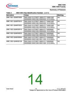
| 型号: | XMC1302-T038X0128 |
| PDF下载: | 下载PDF文件 查看货源 |
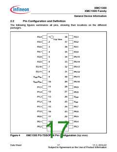
| 内容描述: | [RISC Microcontroller, 32-Bit, FLASH, 33.2MHz, CMOS, PDSO38, TSSOP-38] |
| 分类和应用: | 时钟微控制器光电二极管外围集成电路 |
| 文件页数/大小: | 62 页 / 1898 K |
| 品牌: |  INFINEON [ Infineon ] INFINEON [ Infineon ] |
专业IC领域供求交易平台:提供全面的IC Datasheet资料和资讯,Datasheet 1000万数据,IC品牌1000多家。