XC2287 / XC2286 / XC2285
XC2000 Family Derivatives
Preliminary
General Device Information
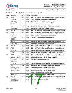
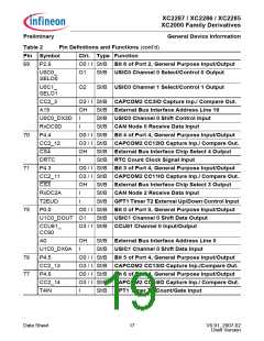
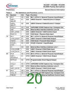
Table 2
Pin Definitions and Functions (cont’d)
Pin Symbol
Ctrl. Type Function
82
P2.9
O0 / I St/B Bit 9 of Port 2, General Purpose Input/Output
U0C1_DOUT O1
St/B USIC0 Channel 1 Shift Data Output
St/B CAN Node 1 Transmit Data Output
TxDC1
CC2_6
A22
O2
O3 / I St/B CAPCOM2 CC6IO Capture Inp./ Compare Out.
OH
St/B External Bus Interface Address Line 22
St/B Clock Signal Input
DIRIN
TCK_A
P0.2
I
I
St/B JTAG Clock Input
83
O0 / I St/B Bit 2 of Port 0, General Purpose Input/Output
U1C0_
O1
St/B USIC1 Channel 0 Shift Clock Output
SCLKOUT
TxDC0
O2
St/B CAN Node 0 Transmit Data Output
CCU61_
CC62
O3 / I St/B CCU61 Channel 2 Input/Output
A2
OH
I
St/B External Bus Interface Address Line 2
St/B USIC1 Channel 0 Shift Clock Input
U1C0_DX1B
P10.0
84
O0 / I St/B Bit 0 of Port 10, General Purpose Input/Output
St/B USIC0 Channel 1 Shift Data Output
U0C1_DOUT O1
CCU60_
CC60
O2 / I St/B CCU60 Channel 0 Input/Output
AD0
OH / I St/B External Bus Interface Address/Data Line 0
U0C0_DX0A
U0C1_DX0A
P3.0
I
I
St/B USIC0 Channel 0 Shift Data Input
St/B USIC0 Channel 1 Shift Data Input
85
O0 / I St/B Bit 0 of Port 3, General Purpose Input/Output
U2C0_DOUT O1
St/B USIC2 Channel 0 Shift Data Output
St/B External Bus Request Output
St/B USIC2 Channel 0 Shift Data Input
St/B CAN Node 3 Receive Data Input
St/B USIC2 Channel 0 Shift Clock Input
BREQ
OH
U2C0_DX0A
RxDC3B
I
I
I
U2C0_DX1A
Data Sheet
19
V0.91, 2007-02
Draft Version

 INFINEON [ Infineon ]