TLE9879QXA40
Electrical Characteristics
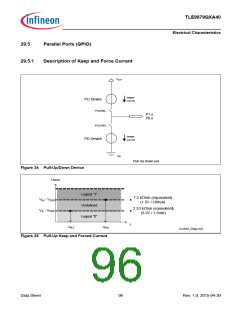
UGPIO
Logical "1"
Undefined
Logical "0"
2.33 kOhm (equivalent)
(3.5V / 1.5mA)
VIH
VIL
7.5 kOhm (equivalent)
(1.5V / 200uA)
I
IPLK
IPLF
Current_Diag-Pull_down.vsd
Figure 36 Pull-Down Keep and Force Current
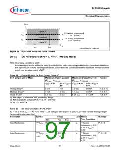
29.5.2
DC Parameters of Port 0, Port 1, TMS and Reset
Note:Operating Conditions apply.
Keeping signal levels within the limits specified in this table ensures operation without overload conditions.
For signal levels outside these specifications, also refer to the specification of the maximum allowed ocurrent
which can be taken out of VDDP.
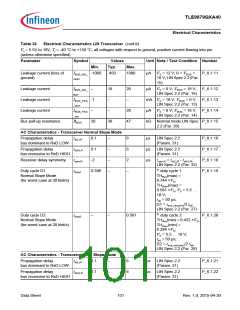
Table 29
Port Output Driver Mode
Current Limits for Port Output Drivers1)
Maximum Output Current
(IOLmax , - IOHmax)
DDP ≥ 4.5V
Maximum Output Current
(IOLnom , - IOHnom)
Number
V
2.6V < VDDP < VDDP ≥ 4.5V 2.6V < VDDP <
4.5V
4.5V
Strong driver2)
Medium driver3)
Weak driver3)
5 mA
3 mA
1.6 mA
1.0 mA
0.25 mA
1.0 mA
0.8 mA
0.15 mA
P_5.1.15
P_5.1.1
P_5.1.2
3 mA
1.8 mA
0.3 mA
0.5 mA
1) Not subject to production test, specified by design.
2) Not available for port pins P0.4, P1.0, P1.1 and P1.2
3) All P0.x and P1.x
Table 30
DC Characteristics Port0, Port1
VS = 5.5 V to 28 V, Tj = -40 °C to +150 °C, all voltages with respect to ground, positive current flowing into pin
(unless otherwise specified)
Parameter
Symbol
Values
Typ.
–
Unit Note /
Test Condition
Number
Min.
HYSP0_P1 0.11 x VDDP
Max.
Input hysteresis
–
V
1) Series
P_5.1.5
resistance = 0 Ω;
4.5V ≤ VDDP
≤
5.5V
Input hysteresis
Data Sheet
HYSP0_P1
–
0.09 x
VDDP
–
V
1) Series
resistance = 0 Ω;
2.6V ≤ VDDP
4.5V
P_5.1.16
_exend
≤
97
Rev. 1.0, 2015-04-30

 INFINEON [ Infineon ]