TLE9879QXA40
10-Bit Analog Digital Converter (ADC1)
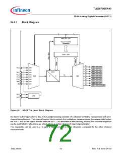
24.2.1
Block Diagram
3
3
/
/
MUX_SEL <2:0>
Channel Controller
(Sequencer)
ADC1 - SFR
10
10
10
10
10
10
10
10
10
/
/
/
/
/
/
/
/
/
ADC1_OUT_CH0
ADC1_OUT_CH1
ADC1_OUT_CH2
ADC1_OUT_CH3
ADC1_OUT_CH4
ADC1_OUT_CH5
ADC1_OUT_CH6
ADC1_OUT_CH7
ADC1_RES_OUT_EIM
P2.0
CH0
CH1
CH2
CH3
ADC1
P2.2
P2.3
P2.4
P2.5
VDH
rfu
10
MUX
A
D
/
MUX
CH4
CH5
CH6
CH7
OP1
OP2
OPA
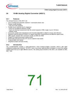
Figure 28
ADC1 Top Level Block Diagram
As shown in the figure above, the ADC1 postprocessing consists of a channel controller (Sequencer) and an 8-
channel demultiplexer. The channel control block controls the multiplexer sequencing on the analog side before
the ADC1 and on the digital domain after the ADC1. As described in the following section, the channel sequence
can be controlled in a flexible way, which allows a certain degree of channel prioritization.
This capability can be used e.g. to give a higher priority to some channels compared to the other channel
measurements.
Data Sheet
72
Rev. 1.0, 2015-04-30

 INFINEON [ Infineon ]