TLE9879QXA40
GPIO Ports and Peripheral I/O
14
GPIO Ports and Peripheral I/O
The TLE9879QXA40 has 15 port pins organized into three parallel ports: Port 0 (P0), Port 1 (P1) and Port 2 (P2).
Each port pin has a pair of internal pull-up and pull-down devices that can be individually enabled or disabled. P0
and P1 are bidirectional and can be used as general purpose input/output (GPIO) or to perform alternate
input/output functions for the on-chip peripherals. When configured as an output, the open drain mode can be
selected. On Port 2 (P2) analog inputs are shared with general purpose input.
14.1
Features
Bidirectional Port Features (P0, P1)
•
•
•
•
•
•
Configurable pin direction
Configurable pull-up/pull-down devices
Configurable open drain mode
Configurable drive strength
Transfer of data through digital inputs and outputs (general purpose I/O)
Alternate input/output for on-chip peripherals
Analog Port Features (P2)
•
•
•
Configurable pull-up/pull-down devices
Transfer of data through digital inputs
Alternate inputs for on-chip peripherals
14.2
Introduction
14.2.1
Port 0 and Port 1
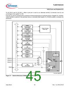
Figure 17 shows the block diagram of an TLE9879QXA40 bidirectional port pin. Each port pin is equipped with a
number of control and data bits, thus enabling very flexible usage of the pin. By defining the contents of the control
register, each individual pin can be configured as an input or an output. The user can also configure each pin as
an open drain pin with or without internal pull-up/pull-down device.
Each bidirectional port pin can be configured for input or output operation. Switching between input and output
mode is accomplished through the register Px_DIR (x = 0 or 1), which enables or disables the output and input
drivers. A port pin can only be configured as either input or output mode at any one time.
In input mode (default after reset), the output driver is switched off (high-impedance). The actual voltage level
present at the port pin is translated into a logic 0 or 1 via a Schmitt trigger device and can be read via the register
Px_DATA.
In output mode, the output driver is activated and drives the value supplied through the multiplexer to the port pin.
In the output driver, each port line can be switched to open drain mode or normal mode (push-pull mode) via the
register Px_OD.
The output multiplexer in front of the output driver enables the port output function to be used for different
purposes. If the pin is used for general purpose output, the multiplexer is switched by software to the data register
Px_DATA. Software can set or clear the bit in Px_DATA and therefore directly influence the state of the port pin.
If an on-chip peripheral uses the pin for output signals, alternate output lines (AltDataOut) can be switched via the
multiplexer to the output driver circuitry. Selection of the alternate output function is defined in registers
Data Sheet
44
Rev. 1.0, 2015-04-30

 INFINEON [ Infineon ]