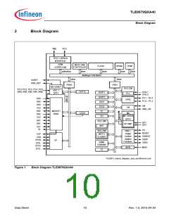
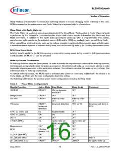
TLE9879QXA40
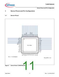
Device Pinout and Pin Configuration
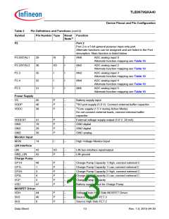
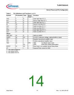
Table 2
Symbol
Pin Definitions and Functions (cont’d)
Pin Number Type
Reset Function
State1)
GH2
7
P
P
P
P
P
P
P
P
–
–
–
–
–
–
–
–
Gate High Side FET 2
Source High Side FET 1
Gate High Side FET 1
Source Low Side FET
Gate Low Side FET 2
Gate Low Side FET 1
Gate High Side FET 3
Gate Low Side FET 3
SH1
8
GH1
9
SL
10
12
13
5
GL2
GL1
GH3
GL3
11
Others
GND_REF
VAREF
OP1
33
34
37
36
20
P
–
GND for VAREF
I/O
–
5V ADC1 reference voltage, optional buffer or input
Negative operational amplifier input
I
I
–
OP2
–
Positive operational amplifier input
TMS
I
I/PD
TMS
Test Mode Select input
I/O
SWD
Serial Wire Debug input/output
RESET
EP
22
–
I/O
–
–
–
Reset input, not available during Sleep Mode
Exposed Pad, connect to GND
1) Only valid for digital IOs
2) Also named VDD5V.
3) Also named VDD1V5.
Data Sheet
14
Rev. 1.0, 2015-04-30

 INFINEON [ Infineon ]