TLE9879QXA40
Device Pinout and Pin Configuration
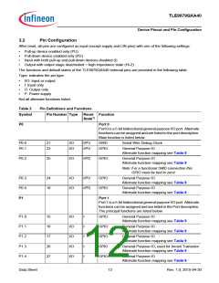
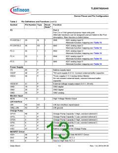
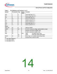
Table 2
Symbol
Pin Definitions and Functions (cont’d)
Pin Number Type
Reset Function
State1)
P2
Port 2
Port 2 is a 5-bit general purpose input-only port.
Alternate functions can be assigned and are listed in the Port
description. Main function is listed below.
P2.0/XTAL1
P2.2/XTAL2
P2.3
29
30
35
32
31
I/I
I
I
I
I
I
AN0
AN2
AN3
AN4
AN5
ADC analog input 0
Alternate function mapping see Table 10
I/O
ADC analog input 2
Alternate function mapping see Table 10
I
I
I
ADC analog input 3
Alternate function mapping see Table 10
P2.4
ADC analog input 4
Alternate function mapping see Table 10
P2.5
ADC analog input 5
Alternate function mapping see Table 10
Power Supply
VS
45
40
38
P
P
P
–
–
–
Battery supply input
2)I/O port supply (5.0 V). Connect external buffer capacitor.
3)Core supply (1.5 V during Active Mode).
Do not connect external loads, connect external buffer
capacitor.
VDDP
VDDC
VDDEXT
GND
41
19
28
39
P
P
P
P
–
–
–
–
External voltage supply output (5.0 V, 20 mA)
GND digital
GND digital
GND analog
GND
GND
Monitor Input
MON
14
I
–
High Voltage Monitor Input
LIN Interface
LIN
43
42
I/O
P
–
–
LIN bus interface input/output
LIN ground
GND_LIN
Charge Pump
CP1H
48
1
P
P
P
P
P
P
–
–
–
–
–
–
Charge Pump Capacity 1 High, connect external C
Charge Pump Capacity 1 Low, connect external C
Charge Pump Capacity 2 High, connect external C
Charge Pump Capacity 2 Low, connect external C
Charge Pump Capacity
CP1L
CP2H
3
CP2L
4
VCP
2
VSD
47
Battery supply input for Charge Pump
MOSFET Driver
VDH
44
46
6
P
P
P
–
–
–
Voltage Drain High Side MOSFET Driver
Source High Side FET 3
SH3
SH2
Source High Side FET 2
Data Sheet
13
Rev. 1.0, 2015-04-30

 INFINEON [ Infineon ]