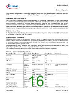
TLE9879QXA40
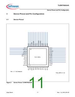
Device Pinout and Pin Configuration
3.2
Pin Configuration
After reset, all pins are configured as input (except supply and LIN pins) with one of the following settings:
•
•
•
•
Pull-up device enabled only (PU)
Pull-down device enabled only (PD)
Input with both pull-up and pull-down devices disabled (I)
Output with output stage deactivated = high impedance state (Hi-Z)
The functions and default states of the TLE9879QXA40 external pins are provided in the following table.
Type: indicates the pin type.
•
•
•
•
I/O: Input or output
I: Input only
O: Output only
P: Power supply
Not all alternate functions listed.
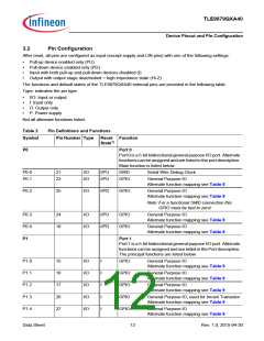
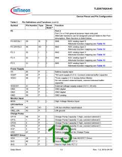
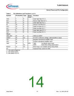
Table 2
Symbol
Pin Definitions and Functions
Pin Number Type
Reset Function
State1)
P0
Port 0
Port 0 is a 5-bit bidirectional general purpose I/O port. Alternate
functions can be assigned and are listed in the port description.
Main function is listed below.
P0.0
P0.1
21
23
I/O
I/O
I/PU
I/PU
SWD
GPIO
Serial Wire Debug Clock
General Purpose IO
Alternate function mapping see Table 8
P0.2
25
I/O
I/PD
GPIO
General Purpose IO
Alternate function mapping see Table 8
Note: For a functional SWD connection this
GPIO must be tied to zero!
P0.3
P0.4
P1
24
18
I/O
I/O
I/PU
I/PD
GPIO
GPIO
Port 1
General Purpose IO
Alternate function mapping see Table 8
General Purpose IO
Alternate function mapping see Table 8
Port 1 is a 5-bit bidirectional general purpose I/O port. Alternate
functions can be assigned and are listed in the Port description.
The principal functions are listed below.
P1.0
P1.1
P1.2
P1.3
P1.4
15
16
17
26
27
I/O
I/O
I/O
I/O
I/O
I
I
I
I
I
GPIO
GPIO
GPIO
GPIO
GPIO
General Purpose IO
Alternate function mapping see Table 9
General Purpose IO
Alternate function mapping see Table 9
General Purpose IO
Alternate function mapping see Table 9
General Purpose IO, used for Inrush Transistor
Alternate function mapping see Table 9
General Purpose IO
Alternate function mapping see Table 9
Data Sheet
12
Rev. 1.0, 2015-04-30

 INFINEON [ Infineon ]