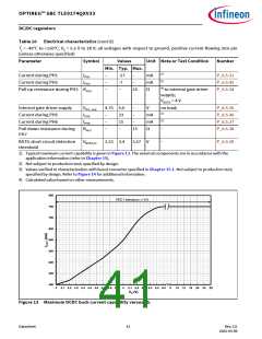
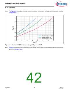
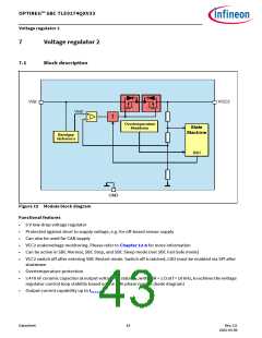
OPTIREG™ SBC TLE9274QXV33
Voltage regulator 2
7.3
Electrical characteristics
Table 11 Electrical characteristics
Tj = -40°C to +150°C; VS2 = 5.5 V to 28 V; all voltages with respect to ground, positive current flowing into pin
(unless otherwise specified)
Parameter
Symbol
Values
Unit Note or
Test Condition
Number
Min. Typ. Max.
Output voltage including line VCC2,out1 4.9
and load regulation
5.0
5.1
V
1) SBC Normal mode P_7.3.1
10 µA < IVCC2 < 100 mA
6.5 V < VS2 < 28 V
Output voltage including line VCC2,out2 4.9
and load regulation
5.0
5.1
V
1) SBC Normal mode P_7.3.2
10 µA < IVCC2 < 80 mA
6 V < VS2 < 28 V
Output voltage including line VCC2,out3 4.85 5.0
and load regulation
5.15
5.07
V
V
1) 10 µA < IVCC2 < 60 mA P_7.3.19
SBC Normal mode
2) SBC Normal mode P_7.3.18
8 V < VS2 < 18 V
Output voltage including line VCC2,out4 4.97
–
and load regulation
10 µA < IVCC2 < 5 mA
25°C< Tj <125°C
Output voltage including line VCC2,out5 4.9
and load regulation
5.05 5.2
V
V
SBC Stop, Sleep mode P_7.3.3
1 mA < IVCC2 < 3 mA
Output voltage including line VCC2,out6 4.9
5.05 5.25
SBC Stop, Sleep mode P_7.3.20
and load regulation
10 µA < IVCC2 < 1 mA
Output drop
VCC2,d1
–
–
–
500 mV
7502) mA
IVCC2 = 30 mA
S2 = 5 V
P_7.3.4
V
Overcurrent limitation
IVCC2,lim
100
current flowing out of P_7.3.5
pin
V
V
CC2 = 0 V
S2 = 13.5 V
1) In SBC Stop mode, the specified output voltage tolerance applies from ICC2 > 3 mA but with increased current
consumption.
2) Not subject to production test, specified by design.
Datasheet
45
Rev.2.0
2022-05-06

 INFINEON [ Infineon ]