TLE9263QX
External Voltage Regulator 3
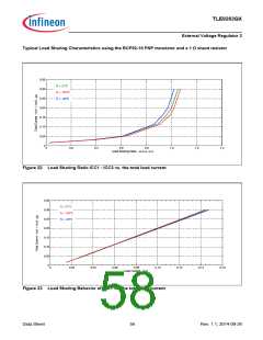
8.6
Electrical Characteristics
VS = 5.5 V to 28 V; Tj = -40 °C to +150 °C; SBC Normal Mode; all outputs open; all voltages with respect to ground;
positive current defined flowing into pin; unless otherwise specified.
Table 14
Electrical Characteristics
Symbol
Parameter
Values
Unit Note / Test Condition
Number
Min.
Typ. Max.
Parameters independent from Test Set-up
External Regulator Control
Drive Current Capability
IVCC3base
40
0
60
3
80
10
10
310
5
mA
µA
V
VCC3base = 13.5 V
VCC3ref = 5 V
P_8.6.1
P_8.6.2
P_8.6.3
P_8.6.6
P_8.6.7
P_8.6.8
P_8.6.9
Input Current VCC3ref
IVCC3ref
V
Input Current VCC3
Shunt Pin
IVCC3shunt
0
3
µA
VVCC3shunt = VS
1)
Output Current Shunt
Voltage Threshold
Vshunt_threshold 180
245
–
mV
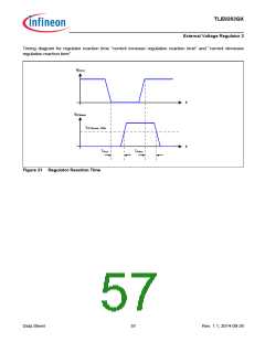
Current increase regulation trIinc
reaction time
–
–
–
µs 4)VCC3 = 6 V to 0 V;
I
CC3base = 20 mA Figure 21
Current decrease regulation trIdec
reaction time
–
5
µs 4)VCC3 = 0 V to 6 V;
I
CC3base = 20 mA Figure 21
Leakage current of
VCC3base when VCC3
disabled
IVCC3base_lk
–
5
µA
VCC3base = VS;
Tj = 25°C
Leakage current of VCC3shunt IVCC3shunt_lk
when VCC3 disabled
–
–
5
µA
V
CC3shunt = VS;
Tj = 25°C
CC3 = OFF;
P_8.6.11
P_8.6.12
P_8.6.33
Base to emitter resistor
RBE
120
–
150
50
185
65
kꢀ
V
Active Peak Threshold VCC3 IVCC3base,Ipeak,r
(Transition threshold
µA 4)Drive current IVCC3base
VCC3base rising
;
I
between low-power and high-
power mode regulator)
VS =13.5V;
-40°C < Tj < 150°C
Active Peak Threshold VCC3 IVCC3base,Ipeak,f 15
(Transition threshold
between high-power and low-
power mode regulator)
30
–
µA 4)Drive current IVCC3base
;
P_8.6.34
P_8.6.13
I
VCC3base falling
VS =13.5V;
-40°C < Tj < 150°C
Parameters dependent on the Test Set-up (with external PNP device MJD-253)
External Regulator Output
Voltage (VCC3 = 5.0V)
VCC3.out1
4.9
5
5.1
V
2)SBC Normal Mode;
load sharing configuration
with 470 mꢀ shunt
resistor;
10 µA < IVCC1 + IVCC3
< 300 mA;
External Regulator Output
Voltage
(VCC3 = 5.0V)
VCC3,out2
4.9
5
5.1
V
2)SBC Normal Mode;
stand-alone configuration
10 mA < IVCC3 < 300 mA;
P_8.6.14
Data Sheet
54
Rev. 1.1, 2014-09-26

 INFINEON [ Infineon ]