TLE9263QX
External Voltage Regulator 3
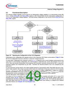
8.2
Functional Description
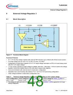
The external voltage regulator can be used as an independent voltage regulator or in load-sharing mode with
VCC1. Setting VCC3_ON in the M_S_CTRL register in SBC Normal Mode sets the stand-alone configuration of
VCC3 as an independent voltage regulator. The load sharing configuration is set via the SPI bit VCC3_LS in the
HW_CTRL register.
VCC3
load sharing?
Default value of
VCC3_LS = ‘0'
No
VCC3
output voltage
in stand-alone
configuration
Yes
5.0V
3.3V
Set bit
Set bit
Set bit
VCC3_LS = 1
VCC3_V_CFG = 0
VCC3_V_CFG = 1
VCC3_V_CFG is
automatically set to 0
Set bit
Set bit
VCC3_ON = 0 or 1
VCC3_ON = 0 or 1
VCC3_LS, VCC3_ON and
VCC3_V_CFG cannot be
changed anymore
VCC3_LS and VCC3_V_CFG
cannot be changed anymore
(once VCC3_ON is set for the first time)
stand-alone
configuration
VCC3 = 5V
stand-alone
configuration
VCC3 = 3.3V
VCC3 load sharing
VCC3 = VCC1
Figure 18 Selecting the Configuration of the VCC3 Regulator
Depending on the configuration the regulator will act in the respective SBC Mode as described in Table 12. After
the VCC3 configuration has been selected, it cannot be changed anymore.
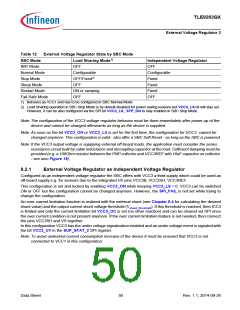
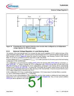
In stand-alone configuration the maximum current ICC3max is defined by the current limitation determined by the
used shunt. In load sharing configuration, the shunt is used to determine the current ratio between VCC1 and
VCC3. Since the junction temperature of the external PNP transistor cannot be sensed by the SBC, it cannot be
protected against over temperature by the SBC. Therefore the thermal behavior has to be analyzed by the
application.
For low-quiescent current reasons, the output voltage tolerance is decreased in SBC Stop Mode because a low-
power mode regulator with a lower accuracy will be active for small loads. If the base current on VCC3 exceeds
IVCC3base > IVCC3base,Ipeak,r then the high-power mode regulator is enabled additionally to support an optimum
dynamic load behavior. If the base current on VCC3 falls below the threshold (IVCC3base < IVCC3base,Ipeak,f), then the
low-quiescent current consumption is resumed again by disabling the high-power mode regulator.
Only the high-power mode regulator is active in SBC Normal Mode.
The status of VCC3 is reported in the SUP_STAT_2 SPI register. The regulator will switch OFF in case of VS
dropping below VS_UV regardless of the VCC3 configuration and will be automatically enabled again when
exceeding this threshold voltage unless the control bit VCC3_VS_ UV_OFF is set. VCC3 will also stay active in
SBC Stop Mode when the bit VCC3_LS_ STP_ON is set and when load sharing is configured (for detailed
protection features see Chapter 15.7 and Chapter 16.3).
Data Sheet
49
Rev. 1.1, 2014-09-26

 INFINEON [ Infineon ]