TLE 6244X
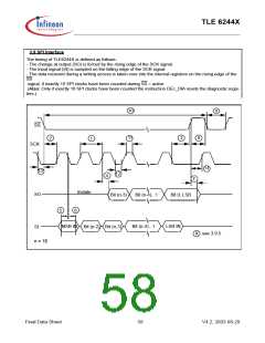
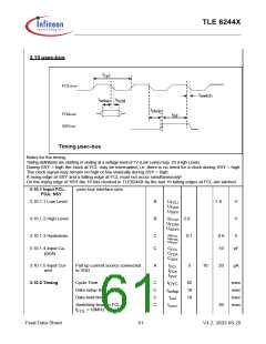
3.10 µsec-bus
t
cyc
FCL/IN16
t
switch
t
t
setup
hold
t
shold
FDA/IN6
SSY/IN7
t
SF
Timing µsec-bus
Notes for the timing:
Timing definitions are starting or ending at a voltage level of 1V (Low Level) resp. 2V (High Level).
During SSY = high the clock at FCL may be interrupted, i.e. there is no need for a clock during SSY = high.
The clock signal may remain on high or low statically during SSY = high.
A rising edge at SSY and a falling edge at FCL must not occur simultaneously!
On the rising edge of SSY the 16 bits clocked in TLE6244X by the last 16 falling edges at FCL are latched.
3.10.1 Input FCL,
FDA, SSY
µsec-bus interface pins
3.10.1.1 Low Level
3.10.1.2 High Level
3.10.1.3 Hysteresis
B
B
UFCLl
UFDAl
USSYl
1.0
V
V
UFCLh 2.0
UFDAh
USSYh
∆U
C
C
FCL
FDA
SSY
0.1
0.6
V
∆U
∆U
3.10.1.4 Input Ca-
pacity
CFCL
CFDA
CSSY
10
20
pF
3.10.1.5 Input Cur-
rent
Pull up current source connected
to VDD
A
IFCL
IFDA
ISSY
5
10
µA
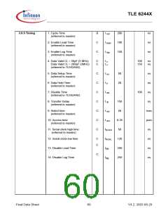
3.10.2 Timing
Cycle Time
C
C
C
C
t
62
10
10
nsec
nsec
nsec
nsec
CYC
Data setup time
Data hold time
t
setup
thold
Switching time on FCL
tswitch
30
f
< 10MHz
FCL
Final Data Sheet
61
V4.2, 2003-08-29

 INFINEON [ Infineon ]