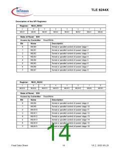
TLE 6244X
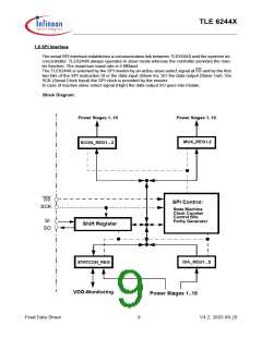
A SPI communication always starts with a SPI instruction sent from the controller to TLE6244X.
During a write cycle the controller sends the data after the SPI instruction, beginning with the MSB.
During a reading cycle, after having received the SPI instruction, TLE6244X sends the correspond-
ing data to the controller, also starting with the MSB.
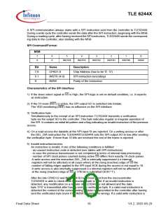
SPI Command/Format:
MSB
7
6
5
4
3
2
1
0
0
0
INSTR4
INSTR3
INSTR2
INSTR1
INSTR0
INSW
Bit
7,6
5-1
0
Name
Description
CPAD1,0
Chip Address (has to be ‘0’, ‘0’)
SPI instruction (encoding)
Parity of the instruction
INSTR (4-0)
INSW
Characteristics of the SPI Interface:
1) If the slave select signal at SS is High, the SPI-logic is set on default condition, i.e. it expects
an instruction.
2) If the 5V-reset (RST) is active, the SPI output SO is switched into tristate.
The VDD monitoring (ABE) has no influence on the SPI interface.
3) Verification byte:
Simultaneously to the receipt of an SPI instruction TLE6244X transmits a verification
byte via the output SO to the controller. This byte indicates regular or irregular operation of
the SPI. It contains an initial bit pattern and a flag indicating an invalid instruction of the previous
access.
4) On a read access the databits at the SPI input SI are rejected. On a writing access or after
the DEL_DIA instruction the TLE6244XTLE6244X sets the SPI output SO to low after sending
the verification byte. If more than 16 bits are received the rest of the frame is rejected.
5) Invalid instruction/access:
An instruction is invalid, if one of the following conditions is fulfilled:
- an unused instruction code is detected (see tables with SPI instructions)
- in case the previous transmission is not completed in terms of internal data processing
- number of SPI clock pulses counted during active SS differs from exactly 16 clock pulses.
A write access and the instruction DEL_DIA is internally suppressed (i.e internal
registers will not be affected) in all cases where at the rising (inactive) edge of SS the
number of falling edges applied to the SPI input SCK during the access is not equal to 16.
A write access is also internally suppressed (i.e internal registers will not be affected) if
at the rising (inactive) edge of SS a 17th bit is submitted (SCK=‘1’).
After the bits CPAD1,0 and INSTR (4-0) have been sent from the microcontroller
TLE6244X is able to check if the instruction code is valid. If an invalid instruction is
detected, any modification on a register of TLE6244X is not allowed and the data
byte ‘FFh’ is transmitted after having sent the verification byte. If a valid read instruction is
detected the content of the corresponding register is transmitted to the controller after having
sent the verification byte (even if bit INSW afterwards is wrong). If a valid write instruction is
Final Data Sheet
10
V4.2, 2003-08-29

 INFINEON [ Infineon ]