TDA5235
Functional Description
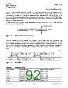
The SPI also includes a safety feature by which the checksum is calculated with an
XOR operation from the address and the data when writing SFR registers. The
checksum is in fact an XOR of the data 8-bitwise after every 8 bits of the SPI write
command. The calculated checksum value is automatically written in the SPICHKSUM
register and can be compared with the expected value. After the SPICHKSUM register
is read, its value is cleared.
In case of an SPI Burst Write frame, a checksum is calculated from the SPI start address
and consecutive data fields.
enable every 8 bit
read/clear
SPI shift register
XOR
Checksum SFR
Figure 63
SPI Checksum Generation
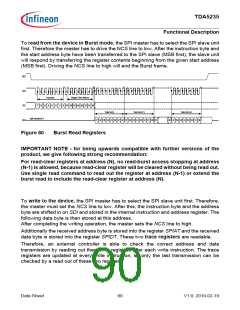
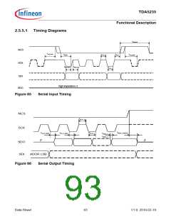
To read the FIFO, the SPI master has to select the SPI slave unit first. Therefore, the
master must set the NCS line to low. After this, the instruction byte is shifted in on SDI
and stored in the internal instruction register. The data bits of the FIFO are then shifted
out on SDO. The following byte is a status word that contains the number of valid bits in
the data packet. After completing the read operation, the master sets the NCS line to
high.
NCS
Frame
Frame
1
8
1
32
1
8
1
8
1
32
1
8
SCK
SDI
Instruction
Instruction
I7 I6
I1 I0
I7 I6
I1 I0
32 FIFO Bits
Status Word
32 FIFO Bits
Status Word
high impedance Z
D0
D1
D30 D31 S7
S6
S1
S0
D0
D1
D30 D31 S7
S6
S1
S0
SDO
Figure 64
Read FIFO
Table 4
Instruction
WR
Instruction Set
Description
Instruction Format
0000 0010
Write to chip
RD
Read from chip
Read FIFO from chip
Write to chip in Burst mode
0000 0011
RDF
0000 0100
WRB
0000 0001
RDB
Read from chip in Burst mode 0000 0101
Data Sheet
92
V1.0, 2010-02-19

 INFINEON [ Infineon ]