TDA5235
Functional Description
NCS
Frame
Frame
1
8
1
8
1
8
1
8
1
8
1
8
SCK
SDI
Instruction
Register Address
Data Byte
Instruction
Register Address
Data Byte
I7 I6 I5 I4 I3 I2 I1 I0 A7 A6 A5 A4 A3 A2 A1 A0 D7 D6 D5 D4 D3 D2 D1 D0
I7 I6 I5 I4 I3 I2 I1 I0 A7 A6 A5 A4 A3 A2 A1 A0 D7 D6 D5 D4 D3 D2 D1 D0
high impedance Z
SDO
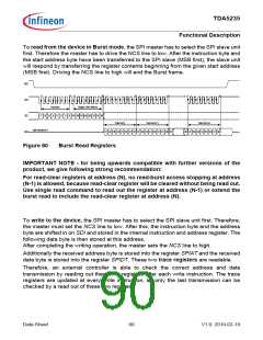
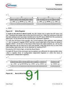
Figure 61
Write Register
To write to the device in Burst mode, the SPI master has to select the SPI slave unit
first. Therefore the master has to drive the NCS line to low. After the instruction byte and
the start address byte have been transferred to the SPI slave (MSB first) the successive
data bytes will be stored into the automatically addressed registers.
To verify the SPI Burst Write transfer, the current address (start address, start address
+ 1, etc.) is stored in register SPIAT and the current data field of the frame is stored in
register SPIDT. At the end of the Burst Write frame the latest address as well as the
latest data field can be read out to verify the transfer. Note that some error in one of the
intermediate data bytes can not be detected by reading SPIDT.
Driving the NCS line to high will end the Burst frame.
A single SPI Burst Write command can be applied very efficiently for data transfer either
within a register block of configuration dependent registers or within the block of
configuration independent registers.
NCS
1
8
1
8
1
8
1
8
1
8
SCK
SDI
Instruction
Register Start Address
Data Byte (i)
Data Byte (i+1)
Data Byte (i+x)
I7 I6 I5 I4 I3 I2 I1 I0 A7 A6 A5 A4 A3 A2 A1 A0 D7 D6 D5 D4 D3 D2 D1 D0 D7 D6 D5 D4 D3 D2 D1 D0
D7 D6 D5 D4 D3 D2 D1 D0
high impedance Z
SDO
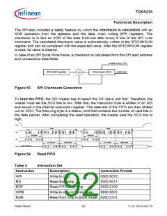
Figure 62
Burst Write Registers
Data Sheet
91
V1.0, 2010-02-19

 INFINEON [ Infineon ]