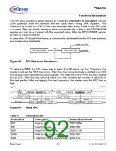
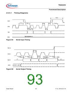
TDA5235
Functional Description
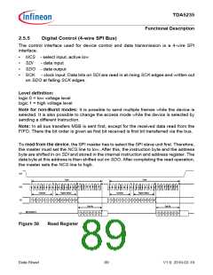
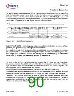
To read from the device in Burst mode, the SPI master has to select the SPI slave unit
first. Therefore the master has to drive the NCS line to low. After the instruction byte and
the start address byte have been transferred to the SPI slave (MSB first), the slave unit
will respond by transferring the register contents beginning from the given start address
(MSB first). Driving the NCS line to high will end the Burst frame.
NCS
1
8
1
8
1
8
1
8
1
8
SCK
SDI
Instruction
Register Start Address
I7 I6 I5 I4 I3 I2 I1 I0 A7 A6 A5 A4 A3 A2 A1 A0
Data Out(i)
Data Out (i+1)
Data Out (i+x)
high impedance Z
SDO
D7 D6 D5 D4 D3 D2 D1 D0 D7 D6 D5 D4 D3 D2 D1 D0 D7
D0 D7 D6 D5 D4 D3 D2 D1 D0
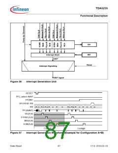
Figure 60
Burst Read Registers
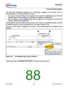
IMPORTANT NOTE - for being upwards compatible with further versions of the
product, we give following strong recommendation:
For read-clear registers at address (N), no read-burst access stopping at address
(N-1) is allowed, because read-clear register will be cleared without being read out.
Use single read command to read out the register at address (N-1) or extend the
burst read to include the read-clear register at address (N).
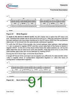
To write to the device, the SPI master has to select the SPI slave unit first. Therefore,
the master must set the NCS line to low. After this, the instruction byte and the address
byte are shifted in on SDI and stored in the internal instruction and address register. The
following data byte is then stored at this address.
After completing the writing operation, the master sets the NCS line to high.
Additionally the received address byte is stored into the register SPIAT and the received
data byte is stored into the register SPIDT. These two trace registers are readable.
Therefore, an external controller is able to check the correct address and data
transmission by reading out these two registers after each write instruction. The trace
registers are updated at every write instruction, so only the last transmission can be
checked by a read out of these two registers.
Data Sheet
90
V1.0, 2010-02-19

 INFINEON [ Infineon ]