TDA5235
Functional Description
first following bits. Therefore the selected default value is a good compromise between
fast symbol synchronization and accuracy/performance.
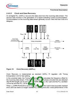
Duty cycle and data rate acceptance limits are adjustable via registers. After locking, the
clock must be stable and must follow the reference input. Therefore, a rapid settling
procedure (Timing Extrapolation Unit) and a slow PLL are implemented.
If the PLL is locked, the reference signal from the Clock Recovery Slicer is used in the
phase detector block to compute the actual error. The error is used in the PI loop filter to
set the digital controlled oscillator running frequency. For the P, I and Timing
Extrapolation Unit settings, the default values for the x_CDRP and x_CDRI control
registers are recommended.
The PLL will be unlocked, if a code violation of more than the defined length is detected,
which is set in the x_TVWIN control register. Another criterion for PLL resynchronization
is an End Of Message (EOM) signalled by the Framer block.
The PLL oscillator generates the chip clock (2 * fdata).
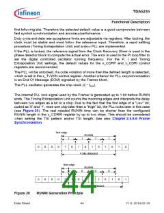
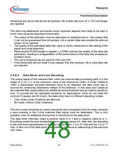
The internal PLL lock signal used by the Framer is generated up to 1 bit before RUNIN
ends. The Timing Extrapolation Unit counts the incoming edges and interprets the delay
between two edges as a bit or a chip. Due to the fact that the first edge of a “Low” bit,
coded as ’0’ and ’1’, rises one chip later than a “High” bit, the PLL locks later in this case
(see Figure 20). The real needed RUNIN time can be shorter than the configured
RUNIN length in the x_CDRRI register by up to two chips. This should be considered
when setting the TSI pattern and/or TSI length. See also Chapter 2.4.8.6 Frame
Synchronization.
first edge
RUNIN
1
1
1
1
0
0
0
0
1
0
1
0
1
0
1
0
1
0
4 bits detected
first edge
0
RUNIN
0
0
0
0
0
0
0
0
1
0
1
0
1
0
1
0
1
4 bits detected
Figure 20
RUNIN Generation Principle
Data Sheet
44
V1.0, 2010-02-19

 INFINEON [ Infineon ]