TDA5235
Functional Description
2.4.6
ASK and FSK Demodulator
AFC track/freeze
AFC
RF PLL ctrl
loop filter
B = 50..300kHz
image suppression /
band limitation (noise)
FSK/ASK
Rate adapter
channel filter FM limiter
FSK
Demodulated
Data
PPF2
BP
Bypass
Rate doubler
Decimation
33 / 46 / 65 / 93 / 132 /
190 / 239 / 282 kHz
(2sided PDF BW)
2nd
conversion
RSSI
8 … 16 samples/chip
(data rate dependent )
Temp
VDDD/2
delog
AGC
RSSI Slope
RSSI Offset
Dig. Gain
Control
Peak Memory
Mux
ADC
Filter
ASK
Div
Analog Gain Control
buffer
RSSI Peak
Detector
register
fSystem
RSSIPMF
register
RSSIPWU
register
RSSI
End of config/
channel
RSSIPWU
(internal
signal)
>
WU event
Begin of config/
channel ,
TH, BL, BH
x*WULOT
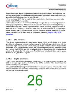
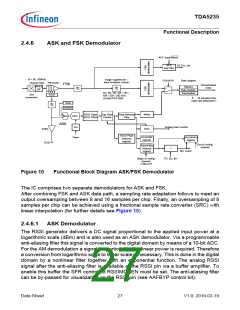
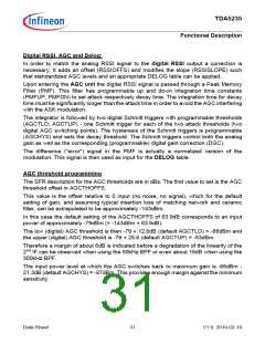
Figure 10
Functional Block Diagram ASK/FSK Demodulator
The IC comprises two separate demodulators for ASK and FSK.
After combining FSK and ASK data path, a sampling rate adaptation follows to meet an
output oversampling between 8 and 16 samples per chip. Finally, an oversampling of 8
samples per chip can be achieved using a fractional sample rate converter (SRC) with
linear interpolation (for further details see Figure 15).
2.4.6.1 ASK Demodulator
The RSSI generator delivers a DC signal proportional to the applied input power at a
logarithmic scale (dBm) and is also used as an ASK demodulator. Via a programmable
anti-aliasing filter this signal is converted to the digital domain by means of a 10-bit ADC.
For the AM demodulation a signal proportional to the linear power is required. Therefore
a conversion from logarithmic scale to linear scale is necessary. This is done in the digital
domain by a nonlinear filter together with an exponential function. The analog RSSI
signal after the anti-aliasing filter is available at the RSSI pin via a buffer amplifier. To
enable this buffer the SFR control bit RSSIMONEN must be set. The anti-aliasing filter
can be by-passed for visualization on the RSSI pin (see AAFBYP control bit).
Data Sheet
27
V1.0, 2010-02-19

 INFINEON [ Infineon ]