TDA5235
Functional Description
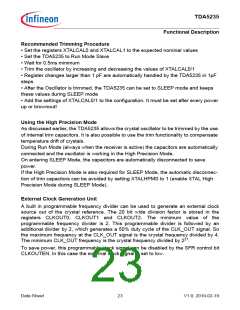
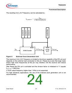
The resulting CLK_OUT frequency can be calculated by:
fsys
fCLKOUT = --------------------------------------------
2 divisionfactor
Enable
Enable
fsys
2 x fCLK_OUT
fCLK_OUT
Divide
by 2
20 Bit Counter
Figure 8
External Clock Generation Unit
The maximum CLK_OUT frequency is limited by the driver capability of the PPx pin and
depends on the external load connected to this pin. Please be aware that large loads
and/or high clock frequencies at this pin may interfere with the receiver and reduce
performance.
After Reset the PPx pin is activated and the division factor is initialized to 11 (equals
fCLK_OUT = 998 kHz).
A clock output frequency higher than 1 MHz is not supported.
For high sensitivity applications, the use of the external clock generation unit is not
recommended.
Data Sheet
24
V1.0, 2010-02-19

 INFINEON [ Infineon ]