TDA5235
Appendix
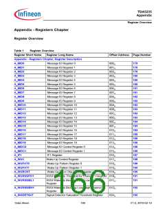
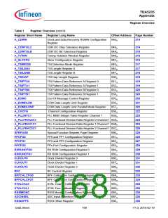
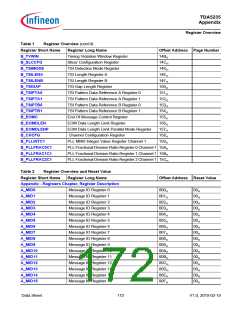
Register Overview
Table 1
Register Overview (cont’d)
Register Short Name
A_CDRRI
Register Long Name
Offset Address Page Number
Clock and Data Recovery RUNIN Configuration
Register
048H
214
A_CDRTOLC
A_CDRTOLB
A_TVWIN
CDR DC Chip Tolerance Register
CDR DC Bit Tolerance Register
Timing Violation Window Register
Slicer Configuration Register
049H
04AH
04BH
04CH
04DH
04EH
04FH
050H
051H
052H
053H
054H
055H
056H
057H
058H
059H
214
215
216
216
217
217
218
218
219
219
220
220
220
221
222
222
223
224
224
225
225
226
227
228
229
230
231
231
232
232
233
234
234
235
235
236
236
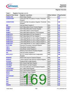
A_SLCCFG
A_TSIMODE
A_TSILENA
A_TSILENB
A_TSIGAP
A_TSIPTA0
A_TSIPTA1
A_TSIPTB0
A_TSIPTB1
A_EOMC
TSI Detection Mode Register
TSI Length Register A
TSI Length Register B
TSI Gap Length Register
TSI Pattern Data Reference A Register 0
TSI Pattern Data Reference A Register 1
TSI Pattern Data Reference B Register 0
TSI Pattern Data Reference B Register 1
End Of Message Control Register
EOM Data Length Limit Register
EOM Data Length Limit Parallel Mode Register
Channel Configuration Register
PLL MMD Integer Value Register Channel 1
A_EOMDLEN
A_EOMDLENP
A_CHCFG
A_PLLINTC1
A_PLLFRAC0C1
A_PLLFRAC1C1
A_PLLFRAC2C1
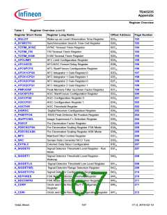
SFRPAGE
PLL Fractional Division Ratio Register 0 Channel 1 05AH
PLL Fractional Division Ratio Register 1 Channel 1 05BH
PLL Fractional Division Ratio Register 2 Channel 1 05CH
Special Function Register Page Register
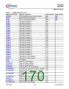
PP0 and PP1 Configuration Register
PP2 and PP3 Configuration Register
PPx Port Configuration Register
RX RUN Configuration Register 0
RX RUN Configuration Register 1
Clock Divider Register 0
080H
081H
082H
083H
084H
085H
086H
087H
088H
089H
08AH
08BH
08CH
08DH
08EH
08FH
090H
PPCFG0
PPCFG1
PPCFG2
RXRUNCFG0
RXRUNCFG1
CLKOUT0
CLKOUT1
Clock Divider Register 1
CLKOUT2
Clock Divider Register 2
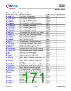
RFC
RF Control Register
BPFCALCFG0
BPFCALCFG1
XTALCAL0
XTALCAL1
RSSIMONC
ADCINSEL
RSSIOFFS
BPF Calibration Configuration Register 0
BPF Calibration Configuration Register 1
XTAL Coarse Calibration Register
XTAL Fine Calibration Register
RSSI Monitor Configuration Register
ADC Input Selection Register
RSSI Offset Register
Data Sheet
168
V1.0, 2010-02-19

 INFINEON [ Infineon ]