TDA5235
Reference
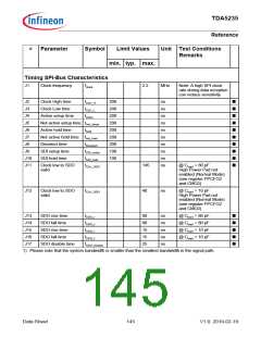
#
Parameter
Symbol
Limit Values
Unit Test Conditions
Remarks
min. typ. max.
Timing SPI-Bus Characteristics
J1
Clock frequency
fclock
2.2
MHz
Note: A high SPI clock
rate during data reception
can reduce sensitivity
J2
Clock High time
Clock Low time
Active setup time
tCLK_H
tCLK_L
tsetup
200
200
200
200
200
200
200
100
100
145
ns
ns
ns
ns
ns
ns
ns
ns
ns
ns
■
■
■
■
■
■
■
■
■
■
J3
J4
J5
Not active setup time tnot_setup
Active hold time thold
Not active hold time tnot_hold
J6
J7
J8
Deselect time
SDI setup time
SDI hold time
tDeselect
tSDI_setup
tSDI_hold
tCLK_SDO
J9
J10
J11
Clock low to SDO
valid
@ Cload = 80 pF
High Power Pad not
enabled (Normal Mode)
(see register PPCFG2
and CMC0)
J12
Clock low to SDO
valid
tCLK_SDO
40
ns
@ Cload = 10 pF
High Power Pad not
enabled (Normal Mode)
(see register PPCFG2
and CMC0)
J13
J14
J15
J16
J17
SDO rise time
SDO fall time
SDO rise time
SDO fall time
SDO disable time
tSDO_r
90
90
15
15
25
ns
ns
ns
ns
ns
@ Cload = 80 pF
@ Cload = 80 pF
@ Cload = 10 pF
@ Cload = 10 pF
■
■
■
■
■
tSDO_f
tSDO_r
tSDO_f
tSDO_disable
1) Please note that the system bandwidth is smaller than the smallest bandwidth in the signal path.
Data Sheet
145
V1.0, 2010-02-19

 INFINEON [ Infineon ]