TDA5235
Reference
#
Parameter
Symbol
Limit Values
Unit Test Conditions
Remarks
min. typ. max.
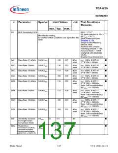
E9
E10
Inband fractional spur
-40
dBc
kHz
■
■
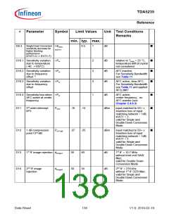
3dB Overall Analog
Frontend Bandwidth
BWANA
230
LNA input to Limiter
output, excluding external
CER filter
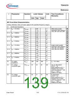
1st IF Buffer Characteristics
F1
F2
F3
Input impedance
Output impedance
Voltage gain
Rin_IF
290
290
3
330
330
4
370
370
5
Ω
fIF = 10...12 MHz
fIF = 10...12 MHz
fIF = 10...12 MHz
■
■
Rout_IF
AVBuffer
Ω
dB
Z
Z
source = 330 Ω
load = 330 Ω
F4
Buffer switch
isolation (CERFSEL)
disolation
60
dB
fIF = 10...12 MHz
see Figure 6
■
■
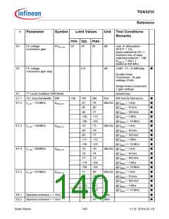
2nd IF Mixer, RSSI and Filter Characteristics
G1
Mixer input
impedance
Rin_IF
290
330
390
Ω
fIF = 10...12 MHz
G2
RSSI
Related to RF input
matched to 50 Ω
G2.1 Dynamic range
(Linearity +/- 2 dB)
DRRSSI
-110
-115
-110
-1
-30
-60
-50
+1
dBm
dBm
dBm
dB
applies for digital RSSI;
AGC on
■
■
■
■
■
applies for analog RSSI
@ 50kHz BPF, AGC off
applies for analog RSSI
@ 300kHz BPF, AGC off
G2.2 Linearity
DRLIN
-95 dBm...-35 dBm;
applies for digital RSSI
G2.3 Temperature drift
within linear dynamic
range
DRTEMP
-2.5
+1.5
dB
-95 dBm...-35 dBm;
applies for digital RSSI
G2.4 Output dynamic
range
VRSSI+
0.8
2.0
+2
12
V
G2.5 analog RSSI error,
untrimmed
DRSSIana -4
dB
at RSSI pin
G2.6 analog RSSI slope,
untrimmed
dVRSSI
dVmix_in
/
8
10
mV/dB at RSSI pin;
typical 600 mV/60 dB =
10 mV/dB
G2.7 digital RSSI error,
untrimmed
DRSSIdig_u -4
+2
dB
RSSI register readout
Data Sheet
141
V1.0, 2010-02-19

 INFINEON [ Infineon ]