TDA 5210
List of Figures
List of Figures
Figure 2-1 P-TSSOP-28-1 package outlines . . . . . . . . . . . . . . . . . . . . . . . . . . . . . . . . . . . . . . . . .
Figure 3-1 IC Pin Configuration . . . . . . . . . . . . . . . . . . . . . . . . . . . . . . . . . . . . . . . . . . . . . . . . . . .
Figure 3-2 Main Block Diagram . . . . . . . . . . . . . . . . . . . . . . . . . . . . . . . . . . . . . . . . . . . . . . . . . . .
Figure 4-1 LNA Automatic Gain Control Circuitry . . . . . . . . . . . . . . . . . . . . . . . . . . . . . . . . . . . . . .
Figure 4-2 RSSI Level and Permissive AGC Threshold Levels . . . . . . . . . . . . . . . . . . . . . . . . . . .
Figure 4-3 Data Filter Design . . . . . . . . . . . . . . . . . . . . . . . . . . . . . . . . . . . . . . . . . . . . . . . . . . . . .
Figure 4-4 Determination of Series Capacitance Value for the Quartz Oscillator . . . . . . . . . . . . . .
Figure 4-5 Data Slicer Threshold Generation with External R-C Integrator . . . . . . . . . . . . . . . . . .
Figure 4-6 Data Slicer Threshold Generation Utilising the Peak Detector . . . . . . . . . . . . . . . . . . .
Figure 4-7 ASK/FSK mode datapath . . . . . . . . . . . . . . . . . . . . . . . . . . . . . . . . . . . . . . . . . . . . . . .
Figure 4-8 Frequency characterstic in case of FSK mode . . . . . . . . . . . . . . . . . . . . . . . . . . . . . . .
2-3
3-2
3-9
4-2
4-3
4-4
4-5
4-7
4-7
4-8
4-9
Figure 4-9 Frequency charcteristic in case of ASK mode . . . . . . . . . . . . . . . . . . . . . . . . . . . . . . . . 4-10
Figure 4-10 Principle of the precharge circuit . . . . . . . . . . . . . . . . . . . . . . . . . . . . . . . . . . . . . . . . . . 4-11
Figure 4-11 Voltage appearing on C2 during precharging process . . . . . . . . . . . . . . . . . . . . . . . . . 4-12
Figure 4-12 Voltage transient on capacitor C attached to pin 20 . . . . . . . . . . . . . . . . . . . . . . . . . . . 4-13
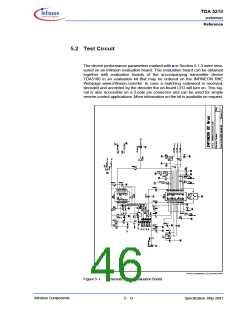
Figure 5-1 Schematic of the Evaluation Board . . . . . . . . . . . . . . . . . . . . . . . . . . . . . . . . . . . . . . . . 5-12
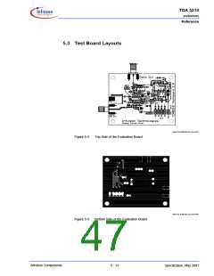
Figure 5-2 Top Side of the Evaluation Board . . . . . . . . . . . . . . . . . . . . . . . . . . . . . . . . . . . . . . . . . 5-13
Figure 5-3 Bottom Side of the Evaluation Board . . . . . . . . . . . . . . . . . . . . . . . . . . . . . . . . . . . . . . . 5-13
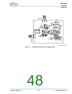
Figure 5-4 Component Placement on the Evaluation Board . . . . . . . . . . . . . . . . . . . . . . . . . . . . . . 5-14
Wireless Components
List of Figures - 1
Specification, May 2001

 INFINEON [ Infineon ]