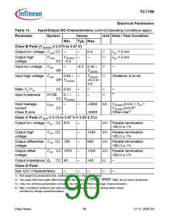
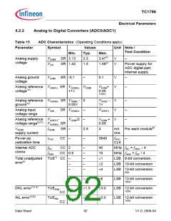
TC1796
Electrical Parameters
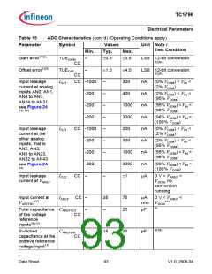
Table 15
ADC Characteristics (cont’d) (Operating Conditions apply)
Parameter
Symbol
Values
Typ.
1
Unit Note /
Test Condition
Min.
–
Max.
1.5
Resistance of the RAREF
reference voltage
input path16)
kΩ
500 Ohm
CC
increased for
AN[1:0] used as
reference input9)
6)9)
Total capacitance CAINTOT
of the analog
–
–
–
–
25
7
pF
pF
CC
CC
inputs16)
9)19)
9)
Switched
CAINSW
capacitance at the
analog voltage
inputs
ON resistance of RAIN
the transmission
gates in the
analog voltage
path
CC –
1
1.5
kΩ
ON resistance for RAIN7T CC 200
300
1000
Ω
Test feature
available only for
AIN79)
the ADC test (pull-
down for AIN7)
Current through
resistance for the
ADC test (pull-
down for AIN7)
IAIN7T CC –
15 rms 30 peak mA Test feature
available only for
AIN79)
1) Voltage overshoot to 4 V are permissible, provided the pulse duration is less than 100 µs and the cumulated
summary of the pulses does not exceed 1 h.
2) Voltage overshoot to 1.7 V are permissible, provided the pulse duration is less than 100 µs and the cumulated
summary of the pulses does not exceed 1 h.
3) A running conversion may become inexact in case of violating the normal operating conditions (voltage
overshoot).
4) If
the
reference
voltage
VAREF
increases
or
the
VDDM
decreases,
so
that
V
AREF = (VDDM + 0.05V to VDDM + 0.07V), then the accuracy of the ADC decreases by 4LSB12.
5) If a reduced reference voltage in a range of VDDM/2 to VDDM is used, then the ADC converter errors increase.
If the reference voltage is reduced with the factor k (k<1), then TUE, DNL, INL Gain and Offset errors increase
with the factor 1/k.
If a reduced reference voltage in a range of 1 V to VDDM/2 is used, then there are additional decrease in the
ADC speed and accuracy.
6) Current peaks of up to 6 mA with a duration of max. 2 ns may occur
7) TUE is tested at VAREF = 3.3 V, VAGND = 0 V and VDDM = 3.3 V
Data Sheet
94
V1.0, 2008-04

 INFINEON [ Infineon ]