TC1796
Electrical Parameters
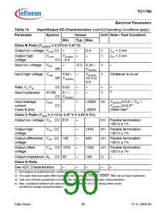
Table 14
Input/Output DC-Characteristics (cont’d)(Operating Conditions apply)
Parameter
Symbol
Values
Unit Note / Test Condition
Min.
Typ. Max.
Class B Pads (VDDEBU = 2.375 to 3.47 V)
Output low voltage VOLB CC –
–
–
0.4
–
V
V
IOL = 2 mA
IOL = 2 mA
Output high
VOHB
VDDEBU
voltage
CC - 0.4
Input low voltage VILB
Input high voltage VIHB
–
-0.3 0.34 ×
V
V
–
SR
VDDEBU
0.64 × –
SR VDDEBU
VDDEBU
+0.3 or
3.6
Whatever is lower
Ratio VIL/VIH
Input hysteresis
CC 0.53
–
–
–
–
–
V
–
5)
HYSB
0.1 ×
CC VDDEBU
Input leakage
current
Class B pins
IOZB
–
–
±3000 nA
±6000
V
V
DDEBU/2-0.6 < VIN <
CC
DDEBU/2+0.66)
Otherwise3)
Class C Pads (VDDP = 3.13 to 3.47 V = 3.3V ± 5%)
Output low voltage VOL CC 815
–
–
–
–
–
mV Parallel termination
100 Ω ± 1%
Output high
voltage
VOH CC
1545
600
mV Parallel termination
100 Ω ± 1%
Output differential VOD CC 150
mV Parallel termination
voltage
100 Ω ± 1%
Output offset
voltage
VOS CC 1075
1325
140
mV Parallel termination
100 Ω ± 1%
Output impedance R0 CC 40
Ω
–
Class D Pads
See ADC Characteristics
–
–
–
–
–
1) Not subject to production test, verified by design / characterization.
2) The pads that have spike-filter function in the input path: PORST, HDRST, NMI, do not have hysteresis.
3) Only one of these parameters is tested, the other is verified by design characterization
4) Max. resistance between pin and next power supply pin 25 Ω for strong driver mode
(verified by design characterization).
Data Sheet
90
V1.0, 2008-04

 INFINEON [ Infineon ]