TC1796
Functional Description
3.10
High-Speed Synchronous Serial Interfaces (SSC0, SSC1)
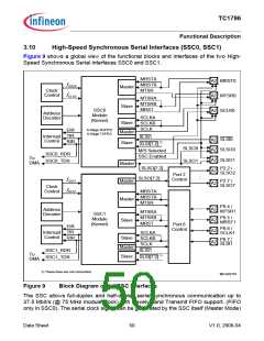
Figure 9 shows a global view of the functional blocks and interfaces of the two High-
Speed Synchronous Serial interfaces SSC0 and SSC1.
MRSTA
MRSTB
MTSR
A2
A2
A2
MRST0
MTSR0
SCLK0
fSSC0
fCLC0
Master
Slave
Clock
Control
MTSRA
MTSRB
MRST
SSC0
Module
(Kernel)
Address
Decoder
SCLKA
SCLKB
SCLK
Slave
8-Stage RXFIFO
8-Stage TXFIFO
EIR
TIR
RIR
Master
Interrupt
Control
SLSI1
SLSI[7:2] 1)
SLSI0
A2
A2
A2
Slave
SLSO0
SLSO1
SLSO0
SLSO1
M/S Selected
SSC Enabled
SSC0_RDR
SSC0_TDR
To
DMA
Master
Master
SLSO[7:2]
SLSO[7:2]
P2.2 /
SLSO2
A2
A2
Port 2
Control
fSSC1
P2.7 /
SLSO7
Clock
Control
fCLC1
MRSTA
MRSTB
MTSR
Master
Slave
P6.4 /
MTSR1
A2
A2
A2
A2
Address
Decoder
MTSRA
MTSRB
MRST
SSC1
Module
(Kernel)
P6.5 /
MRST1
Port 6
Control
EIR
TIR
RIR
P6.6 /
SCLK1
Interrupt
Control
SCLKA
SCLKB
SCLK
Slave
Master
Slave
P6.7 /
SLSI1
SSC1_RDR
SSC1_TDR
SLSI1
SLSI[7:2] 1)
To
DMA
1) These lines are not connected
MCA05791
Figure 9
Block Diagram of the SSC Interfaces
The SSC allows full-duplex and half-duplex serial synchronous communication up to
37.5 Mbit/s (@ 75 MHz module clock) with Receive and Transmit FIFO support. (FIFO
only in SSC0). The serial clock signal can be generated by the SSC itself (Master Mode)
Data Sheet
50
V1.0, 2008-04

 INFINEON [ Infineon ]