TC1796
General Device Information
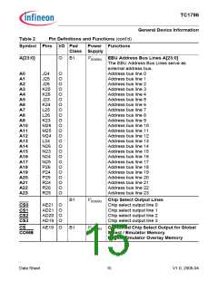
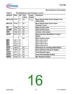
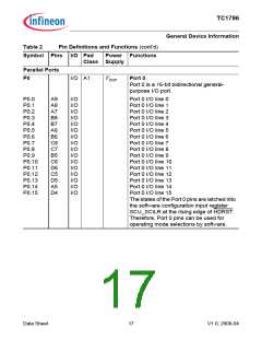
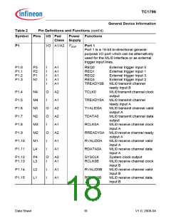
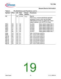
Table 2
Symbol Pins I/O Pad
Class Supply
Pin Definitions and Functions (cont’d)
Power Functions
BFCLKO AF25 O
B2
VDDEBU Burst Mode Flash Clock Output (non-
differential)
BFCLKI AF24 I
B1
Burst Mode Flash Clock Input
(feedback clock)
RD
RD/WR
ADV
AF20 O
AF21 O
AF22 O
AF19 O
B1
B1
B1
B1
Read Control Line
Write Control Line
Address Valid Output
MR/W
Motorola-style Read/Write Control
Signal
B1
Byte Control Lines
Byte control line 0
Byte control line 1
Byte control line 2
Byte control line 3
BC0
BC1
BC2
BC3
AE17 O
AD17 O
AF18 O
AE18 O
WAIT
BAA
HOLD
HLDA
BREQ
AE20 I
AF23 O
AF17 I
AD18 O
AD22 O
B1
B1
B1
B1
B1
Wait Input for inserting Wait-States
Burst Address Advance Output
Hold Request Input
Hold Acknowledge Output
Bus Request Output
Data Sheet
16
V1.0, 2008-04

 INFINEON [ Infineon ]