PDF
最近搜索
热门搜索
发布采购

| 型号: | SAK-TC399XP-256F300S BC |
| PDF下载: | 下载PDF文件 查看货源 |
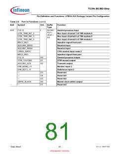
| 内容描述: | [Infineon releases its second generation AURIX microcontroller in embedded flash 40 nm technology. It comes back with an increase in performance, memory sizes, connectivity and more scalability to address the new automotive trends and challenges. This family has more than 20 products to provide the most scalable portfolio of safety microcontroller. In terms of performance, the highest end product TC39x offers 6 cores running at 300 MHz and up to 6.9 MBytes embedded RAM, and consuming below 2 W. ] |
| 分类和应用: | |
| 文件页数/大小: | 548 页 / 21256 K |
| 品牌: |  INFINEON [ Infineon ] INFINEON [ Infineon ] |
专业IC领域供求交易平台:提供全面的IC Datasheet资料和资讯,Datasheet 1000万数据,IC品牌1000多家。