TC39x BC/BD-Step
Pin Definition and Functions: LFBGA-516 Package Variant Pin Configuration
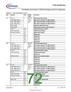
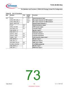
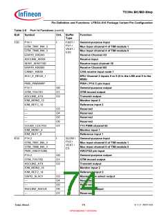
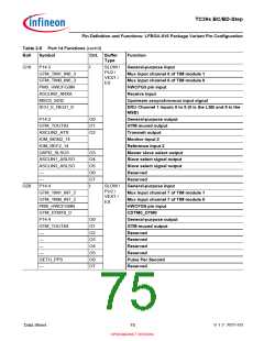
Table 2-7 Port 13 Functions (cont’d)
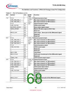
Ball
Symbol
Ctrl. Buffer
Type
Function
A12
P13.13
I
SLOW /
PU1 /
VEXT /
ES
General-purpose input
Mux input channel 0 of TIM module 7
Mux input channel 5 of TIM module 5
Mux input channel 5 of TIM module 3
Injection signal from port
RXD inputs (receive data) channel 3
General-purpose output
GTM muxed output
GTM_TIM7_IN0_3
GTM_TIM5_IN5_5
GTM_TIM3_IN5_9
MSC2_INJ0
PSI5_RX3B
P13.13
O0
O1
O2
O3
O4
O5
O6
O7
I
GTM_TOUT262
ASCLIN7_ASCLK
Shift clock output
—
Reserved
—
Reserved
—
Reserved
—
Reserved
—
Reserved
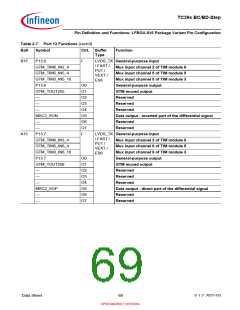
B11
P13.14
SLOW /
PU1 /
VEXT /
ES
General-purpose input
Mux input channel 1 of TIM module 7
Mux input channel 2 of TIM module 5
Mux input channel 2 of TIM module 3
General-purpose output
GTM muxed output
GTM_TIM7_IN1_3
GTM_TIM5_IN2_4
GTM_TIM3_IN2_7
P13.14
O0
O1
O2
O3
O4
O5
O6
O7
I
GTM_TOUT252
—
Reserved
QSPI5_SLSO4
Master slave select output
Reserved
—
—
Reserved
—
Reserved
—
Reserved
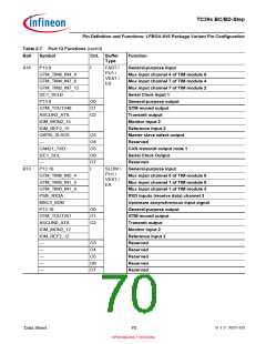
A11
P13.15
SLOW /
PU1 /
VEXT /
ES
General-purpose input
Mux input channel 2 of TIM module 7
Mux input channel 7 of TIM module 5
Mux input channel 7 of TIM module 3
General-purpose output
GTM muxed output
GTM_TIM7_IN2_3
GTM_TIM5_IN7_4
GTM_TIM3_IN7_9
P13.15
O0
O1
O2
O3
O4
O5
O6
O7
GTM_TOUT264
ASCLIN7_ASLSO
Slave select signal output
Reserved
—
PSI5_TX3
TXD outputs (send data)
Reserved
—
—
—
Reserved
Reserved
Data Sheet
72
V 1.2, 2021-03
OPEN MARKET VERSION

 INFINEON [ Infineon ]