TC39x BC/BD-Step
Pin Definition and Functions: LFBGA-516 Package Variant Pin Configuration
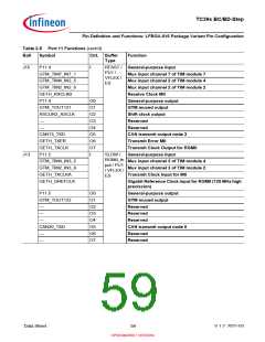
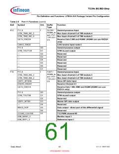
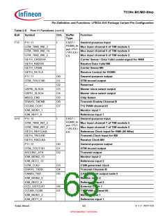
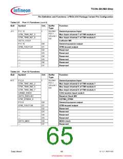
Table 2-5 Port 11 Functions (cont’d)
Ball
Symbol
Ctrl. Buffer
Type
Function
F13
P11.11
I
FAST /
General-purpose input
Mux input channel 6 of TIM module 3
Mux input channel 0 of TIM module 3
Mux input channel 6 of TIM module 2
Carrier Sense / Data Valid combi-signal for RMII
Receive Data Valid MII
Carrier Sense MII
RGMII_In
put / PU1
/ VFLEX /
ES
GTM_TIM3_IN6_2
GTM_TIM3_IN0_14
GTM_TIM2_IN6_2
GETH_CRSDVA
GETH_RXDVA
GETH_CRSB
GETH_RCTLA
P11.11
Receive Control for RGMII
General-purpose output
GTM muxed output
O0
O1
O2
O3
O4
O5
O6
O7
GTM_TOUT100
—
Reserved
QSPI0_SLSO4
QSPI1_SLSO4
MSC0_EN0
Master slave select output
Master slave select output
Chip Select
ERAY0_TXENB
CCU60_CC61
IOM_MON1_1
IOM_REF1_5
P11.12
Transmit Enable Channel B
T12 PWM channel 61
Monitor input 1
Reference input 1
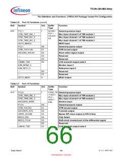
G13
I
FAST /
RGMII_In
put / PU1
/ VFLEX /
ES
General-purpose input
Mux input channel 7 of TIM module 3
Mux input channel 7 of TIM module 2
Reference Clock input for RMII (50 MHz)
Transmit Clock Input for MII
Receive Clock MII
GTM_TIM3_IN7_2
GTM_TIM2_IN7_2
GETH_REFCLKA
GETH_TXCLKB
GETH_RXCLKA
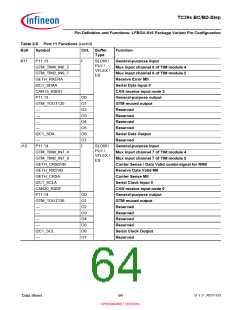
P11.12
O0
O1
O2
General-purpose output
GTM muxed output
GTM_TOUT101
ASCLIN1_ATX
IOM_MON2_13
IOM_REF2_13
GTM_CLK2
Transmit output
Monitor input 2
Reference input 2
O3
O4
O5
CGM generated clock
Transmit Channel B
ERAY0_TXDB
CAN03_TXD
IOM_MON2_8
IOM_REF2_8
CCU_EXTCLK1
CCU60_CC60
IOM_MON1_2
IOM_REF1_6
CAN transmit output node 3
Monitor input 2
Reference input 2
O6
O7
External Clock 1
T12 PWM channel 60
Monitor input 1
Reference input 1
Data Sheet
63
V 1.2, 2021-03
OPEN MARKET VERSION

 INFINEON [ Infineon ]