TC39x BC/BD-Step
Electrical SpecificationEVR
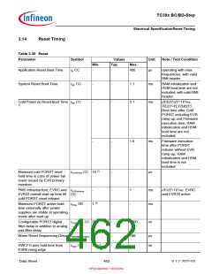
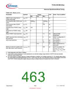
Table 3-31 EVR33 LDO (cont’d)
Parameter
Symbol
Values
Typ.
Unit
Note / Test Condition
Min.
Max.
Line step response
dVout/dVin
CC
-
-
40
mV
dVin/dT=1V/ms; dV=
3.6 to 5V; IMAX=60mA;
ΔVOUTTC is included
-40
-
-
mV
dVin/dT=1V/ms; dV= 5
to 3.6V; IMAX=60mA;
ΔVOUTTC is included
-
-
-
280
-
mV
mV
dVin/dT=50V/ms; dV=
3.6 to 5V; IMAX=60mA
-165
dVin/dT=50V/ms; dV=
5 to 3.6V; IMAX=60mA
1) A maximum pass device dropout voltage of 300mV is included in the minimum input voltage to ensure optimal pass device
performance during normal operation.
2) VEXT Input voltage drop up to 2.97V leading to VDDP3 output voltage drop upto 2.6V can be tolerated if Flash is switched
before to low performance mode.
3) No external inductive load permissible if EVR33 is used.
4) It is also recommended that the resistance of the supply trace from the pin to the EVR output capacitor is less than 100 mOhm.
An additional decoupling capacitor of 100nF shall be located close to the pin before Cout.
5) IMAX is limited to 40 mA incase of Low voltage mode (cranking case) with on chip pass devices. In case EVR33 is not used,
Injection current into 3.3V VDDP3 supply rail with active sink on 5V VEXT rail should be limited to 500 mA if during power
sequencing 3.3V is supplied before 5V by external regulator.
6) EVR is robust against residual voltage ramp-up starting between 0 - 2.97 V. A VEXT voltage ramp range between 0.5V/min
upto 120V/ms is covered in robustness validation. The generated voltage itself follows a soft ramp-up over the tSTR time to
avoid overshoots.
7) Settling time is defined until output voltage is within +-1% of the mean(VOUTT) of the individual device.
Table 3-32 Supply Monitors
Parameter
Symbol
Values
Typ.
Unit
Note / Test Condition
Min.
Max.
Primary Undervoltage Reset
threshold for VDDP3 before
trimming 1)
V
V
RST33 CC
-
-
3.00
V
by reset release before
EVR trimming on
supply ramp-up
Primary undervoltage reset
threshold for VDD before
trimming
RSTC CC
-
-
1.138
V
by reset release before
trimming on supply
ramp-up including 2
LSB voltage Hysteresis
V
EXT primary undervoltage
VEXTPRIUV
2.86
2.92
2.90
1.105
2.97
2.97
1.125
V
V
V
VEXT = Undervoltage
cold PORST Primary
Monitor Threshold
monitor accuracy after trimming CC
2)
VDDP3 primary undervoltage
VDDP3PRIUV 2.86 3)
VDDP3 = Undervoltage
cold PORST Primary
Monitor Threshold
monitor accuracy after trimming CC
2)
VDD primary undervoltage
V
DDPRIUV CC 1.08 3)
VDD = Undervoltage
cold PORST Primary
Monitor Threshold
monitor accuracy after trimming
2)
Data Sheet
466
V 1.2, 2021-03
OPEN MARKET VERSION

 INFINEON [ Infineon ]