TC39x BC/BD-Step
Pin Definition and Functions: LFBGA-516 Package Variant Pin Configuration
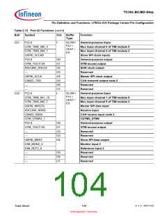
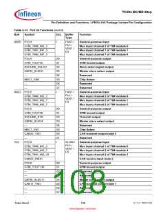
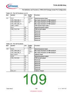
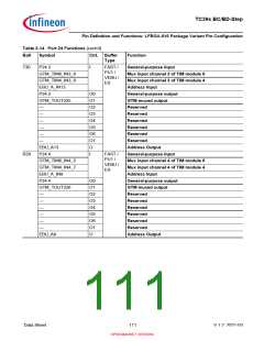
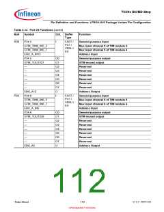
Table 2-13 Port 23 Functions (cont’d)
Ball
Symbol
Ctrl. Buffer
Type
Function
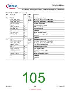
AA25 P23.4
GTM_TIM6_IN3_2
I
FAST /
PU1 /
VEXT /
ES
General-purpose input
Mux input channel 3 of TIM module 6
Mux input channel 7 of TIM module 1
Mux input channel 7 of TIM module 0
General-purpose output
GTM muxed output
GTM_TIM1_IN7_5
GTM_TIM0_IN7_5
P23.4
O0
O1
O2
O3
O4
O5
O6
O7
I
GTM_TOUT45
ASCLIN6_ASLSO
QSPI4_SLSO5
—
Slave select signal output
Master slave select output
Reserved
MSC1_EN0
—
Chip Select
Reserved
—
Reserved
AA22 P23.5
FAST /
PU1 /
VEXT /
ES
General-purpose input
Mux input channel 2 of TIM module 6
Mux input channel 2 of TIM module 1
Mux input channel 2 of TIM module 0
General-purpose output
GTM muxed output
GTM_TIM6_IN2_2
GTM_TIM1_IN2_7
GTM_TIM0_IN2_7
P23.5
O0
O1
O2
O3
O4
O5
O6
O7
I
GTM_TOUT46
ASCLIN6_ATX
QSPI4_SLSO4
—
Transmit output
Master slave select output
Reserved
MSC1_EN1
CAN22_TXD
—
Chip Select
CAN transmit output node 2
Reserved
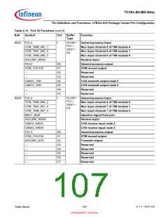
Y22
P23.6
SLOW /
PU1 /
VEXT /
ES
General-purpose input
Mux input channel 1 of TIM module 6
Mux input channel 2 of TIM module 4
Mux input channel 2 of TIM module 1
CAN receive input node 2
General-purpose output
GTM muxed output
GTM_TIM6_IN1_2
GTM_TIM4_IN2_7
GTM_TIM1_IN2_10
CAN22_RXDC
P23.6
O0
O1
O2
O3
O4
O5
O6
O7
GTM_TOUT138
—
Reserved
—
Reserved
QSPI0_SLSO11
CAN11_TXD
—
Master slave select output
CAN transmit output node 1
Reserved
—
Reserved
Data Sheet
108
V 1.2, 2021-03
OPEN MARKET VERSION

 INFINEON [ Infineon ]