TC1767
Introduction
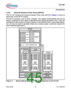
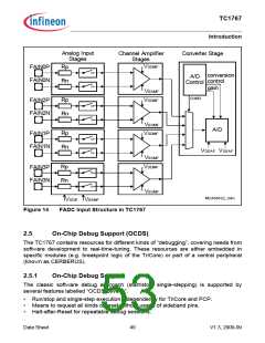
2.4.7
Analog-to-Digital Converters
The TC1767 includes two Analog to Digital Converter modules (ADC0, ADC1) and one
Fast Analog to Digital Converter (FADC).
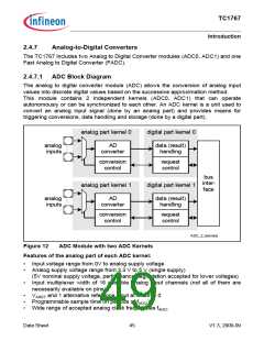
2.4.7.1 ADC Block Diagram
The analog to digital converter module (ADC) allows the conversion of analog input
values into discrete digital values based on the successive approximation method.
This module contains 2 independent kernels (ADC0, ADC1) that can operate
autonomously or can be synchronized to each other. An ADC kernel is a unit used to
convert an analog input signal (done by an analog part) and provides means for
triggering conversions, data handling and storage (done by a digital part).
analog part kernel 0
digital part kernel 0
analog
inputs
AD
converter
data (result)
handling
conversion
control
request
control
bus
inter-
face
analog part kernel 1
digital part kernel 1
analog
inputs
AD
converter
data (result)
handling
conversion
control
request
control
ADC_2_kernels
Figure 12
ADC Module with two ADC Kernels
Features of the analog part of each ADC kernel:
• Input voltage range from 0V to analog supply voltage
• Analog supply voltage range from 3.3 V to 5 V (single supply)
(5V nominal supply voltage, performance degradation accepted for lower voltages)
• Input multiplexer width of 16 possible analog input channels (not all of them are
necessarily available on pins)
• VAREF and 1 alternative reference input at channel 0
• Programmable sample time (in periods of fADCI
)
• Wide range of accepted analog clock frequencies fADCI
Data Sheet
45
V1.3, 2009-09

 INFINEON [ Infineon ]